Uniform axial force applying device for graphical heterogeneous bonding of silicon-based III-V epitaxial material

A III-V, epitaxial material technology, used in electrical components, semiconductor/solid-state device manufacturing, circuits, etc., can solve the problems of wafer parallelism deviation, uneven force, crystal orientation shift, etc., to achieve firm bonding , to achieve the effect of automatic leveling and uniform pressure

Inactive Publication Date: 2012-08-22
INST OF SEMICONDUCTORS - CHINESE ACAD OF SCI
View PDF4 Cites 2 Cited by
  • Summary
  • Abstract
  • Description
  • Claims
  • Application Information

AI Technical Summary

Problems solved by technology

It will lead to two problems: First, even if the force application system is absolutely parallel, if the parallelism of the wafer deviates, the force will be uneven
The

Method used


Image

  • Uniform axial force applying device for graphical heterogeneous bonding of silicon-based III-V epitaxial material
  • Uniform axial force applying device for graphical heterogeneous bonding of silicon-based III-V epitaxial material

Examples


Embodiment Construction

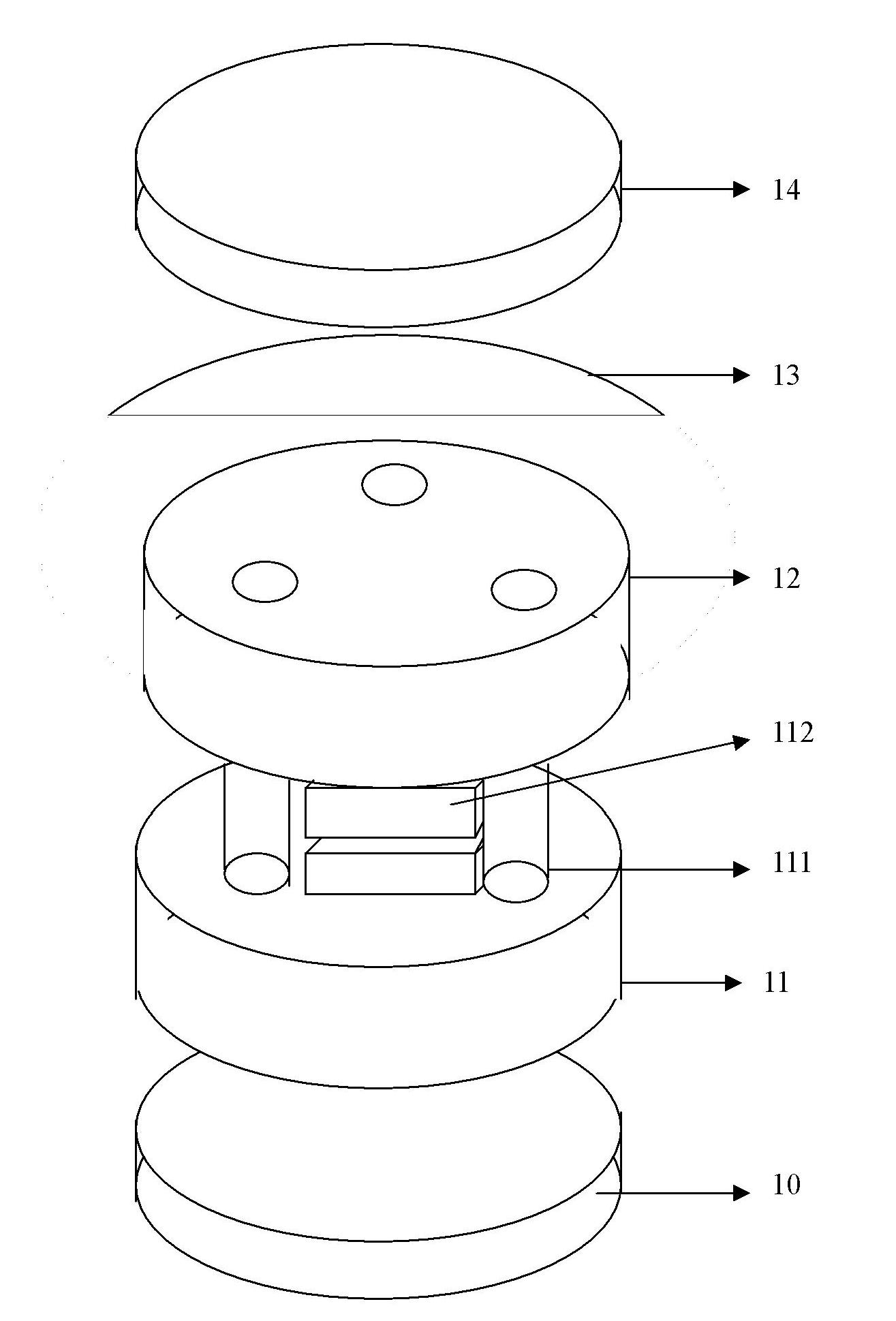
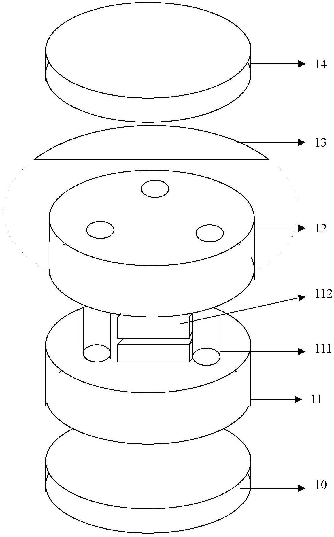
[0020] see figure 1 As shown, the present invention provides a silicon-based III-V epitaxial material pattern heterogeneous bonding uniform axial force applying device, including:

[0021] The lower force application cover plate 10 is in the shape of a disc; the lower force application cover plate 10 will be fixed to the piston end of the upper end cylinder of the bonding equipment through an adjustable connecting part. In the cylinder, the pressure is controlled by the amount of air inflated, and the lower force-applying cover plate 10 is pushed to move or the pressure is changed. The lower force-applying cover plate 10 is made of stainless steel and is polished. It is a pair with the upward force cover plate 14, and the features are the same. The upper and lower force application covers can be adjusted to ensure parallelism.

[0022] Undertake holder 11, this lower accept holder 11 is disc shape, has a plurality of round holes evenly distributed on it (the number of the r...


PUM

PropertyMeasurementUnit
Diameteraaaaaaaaaa
Thicknessaaaaaaaaaa
Thicknessaaaaaaaaaa

Abstract

The invention discloses a uniform axial force applying device for graphical heterogeneous bonding of a silicon-based III-V epitaxial material. The uniform axial force applying device comprises a lower force applying cover plate, a lower bearing support, an upper force applying support, a planoconvex lens and an upper force applying cover plate, wherein the lower force applying cover plate is wafer-shaped; the lower bearing support is wafer-shaped and is positioned on the lower force applying cover plate, and a plurality of round holes are uniformly distributed on the upper surface of the lower bearing support; the upper force applying support is wafer-shaped and is positioned on the lower force bearing support, and a plurality of round holes are uniformly distributed on the upper surface of the upper force applying support; and the lower bearing support and the upper force applying support are connected by a plurality of directional cylinders in an inserting manner; two protective accompanying pieces are also arranged between the lower bearing support and the upper force applying support and are superimposed from top to bottom; the planoconvex lens is positioned on the upper force applying support; and the upper force applying cover plate is wafer-shaped, and is positioned on the planoconvex lens. The uniform axial force applying device has the characteristics that the whole axial pressure applying method does not adopt a direct pressurizing mode, but a leveling part, the force bearing parts and the protective parts are added, so that the uniform pressure applying is realized; and a target chip can bear larger pressure without fragmentation, so that the firmer bonding is realized.

Description

technical field [0001] The invention relates to the technical field of photonic optoelectronic devices and chip manufacturing, in particular to a silicon-based III-V epitaxial material pattern heterogeneous bonding uniform axial force applying device, which is used for mixing silicon-based photon, optoelectronic active and passive Fabrication of devices or chips, suitable for photonic optoelectronic integration applications. Background technique [0002] Silicon-based semiconductors are the cornerstone of the modern microelectronics industry, but they are reaching their limits, especially when it comes to interconnects. However, optoelectronic technology is in a stage of rapid development. Today's semiconductor light-emitting devices are mostly made of compound materials, which are not compatible with silicon microelectronics technology. Therefore, it is meaningful to integrate photonic technology and microelectronic technology to develop silicon-based optoelectronics scienc...

Claims


Application Information

Patent Timeline
IPC IPC(8): H01L21/67H01L21/18
Inventor 张冶金郑婉华渠红伟
Owner INST OF SEMICONDUCTORS - CHINESE ACAD OF SCI
Why Eureka
Try Eureka