Ink-jet head and ink-jet recording apparatus
A technology of inkjet head and nozzle plate, applied in the direction of inking device, printing, etc., can solve the problems that the inkjet head components cannot be significantly dense, and the size of the inkjet head cannot be significantly reduced.
- Summary
- Abstract
- Description
- Claims
- Application Information
AI Technical Summary
Problems solved by technology
Method used
Image
Examples
example 1
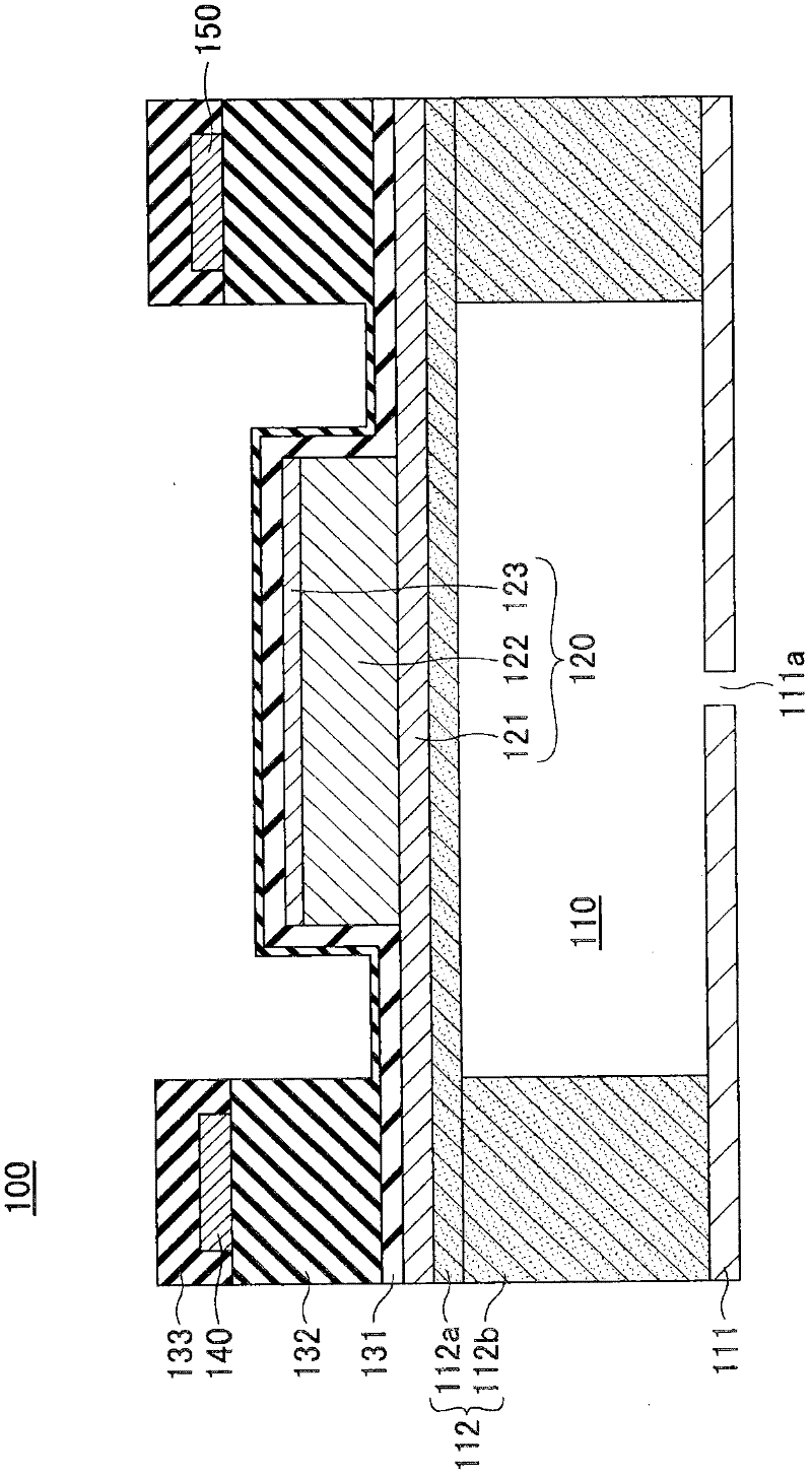
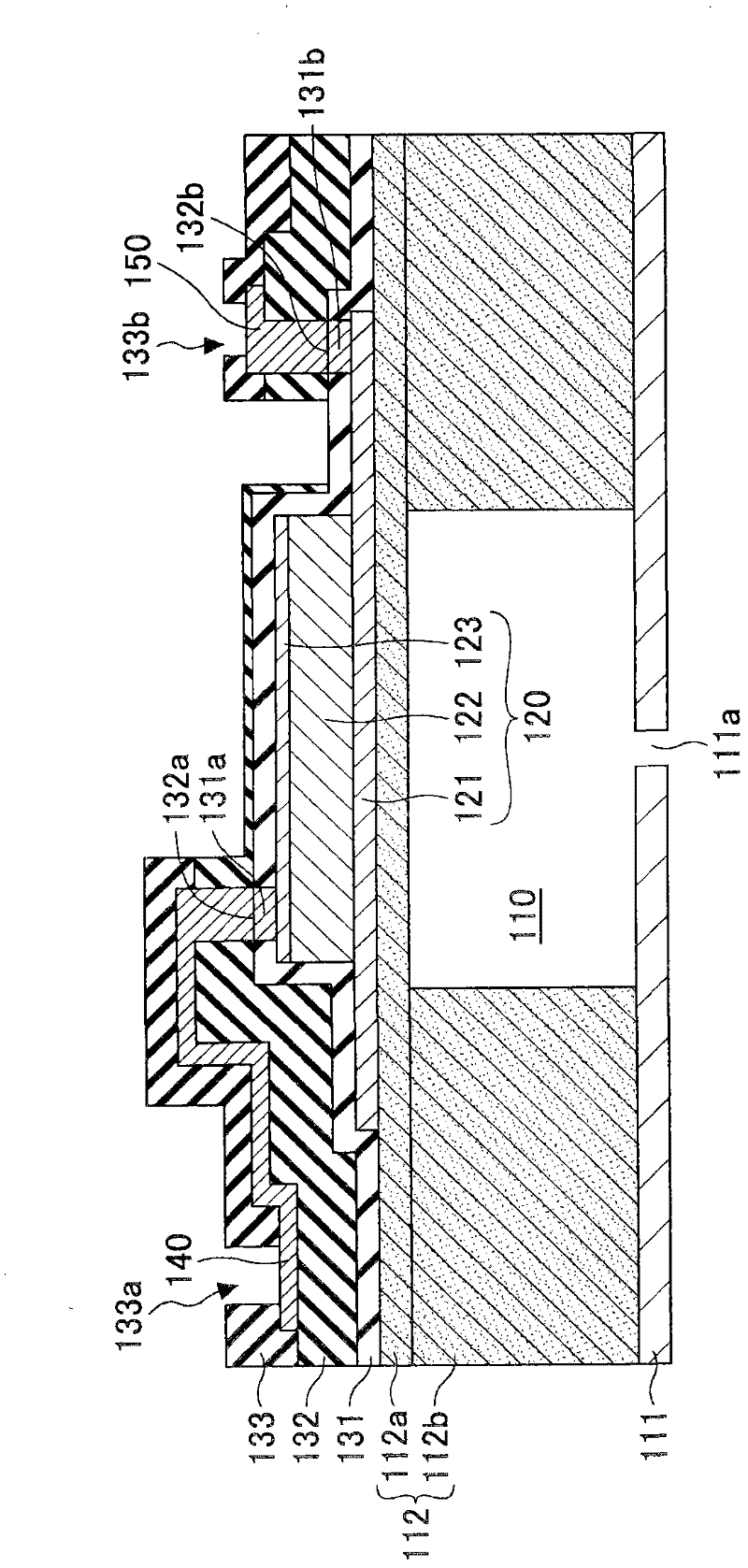
[0084] A thermally oxidized film having a film thickness of 1 µm was formed as a vibrating plate on a silicon wafer having a (100) crystal plane as a main surface. Then, a titanium film having a film thickness of 50 nm, a platinum film having a film thickness of 200 nm, and a SrRuO film having a film thickness of 100 nm were deposited on the thermal oxide film formed on the silicon wafer by a sputtering method.
[0085] Then, coating the PZT precursor solution on the obtained layered product, drying the PZT precursor solution-coated layered product at 120° C., and demarcating the dried layered product at a high temperature of 500° C. were repeated three times. No defects such as cracks were observed on the surface of the obtained film. The obtained d-film was subjected to rapid thermal annealing (RTA) at 700° C. to thermally crystallize it. This RTA was repeated four times to obtain Pb(Zr 0.53 Ti 0.47 )O 3 membrane.
[0086]Next, a layered product formed of a SrRuO film w...
example 2
[0094] An inkjet head was manufactured in the same manner as in Example 1 except that the film thickness of the ZrO film (ie, second insulating film 132 ) was changed to 100 nm. The film thickness of the region of the second insulating film 132 on which the third insulating film 133 is not formed (ie, the second region) is 9 nm.
example 3
[0096] The inkjet head was fabricated in the same manner as in Example 1, except that Al 2 o 3 The film thickness of the film (ie, the first insulating film 131 ) becomes 20 nm. The film thickness of the region of the second insulating film 132 on which the third insulating film 133 is not formed (ie, the second region) is 25 nm.
PUM
 Abstract
Description
Claims
Application Information


