Static discharge protective circuit and display device comprising same

A protection circuit, electrostatic discharge technology, applied in the direction of circuits, static indicators, electrical components, etc., can solve the problems of external drive circuit damage, panel failure, etc.

Active Publication Date: 2012-08-29
BOE TECH GRP CO LTD
View PDF2 Cites 10 Cited by
  • Summary
  • Abstract
  • Description
  • Claims
  • Application Information

AI Technical Summary

Problems solved by technology

Because of this, if the panel is designed with the existing ESD protection circuit structure, then when the panel is working normally, the data (data) line and the gate (gate) li

Method used


Image

  • Static discharge protective circuit and display device comprising same
  • Static discharge protective circuit and display device comprising same
  • Static discharge protective circuit and display device comprising same

Examples


Embodiment Construction

[0014] In order to use the emerging Oxide TFT for electrostatic protection, the present invention provides a corresponding electrostatic protection circuit in combination with the characteristics of the depletion TFT. Embodiments of the present invention will be described below in conjunction with the accompanying drawings.

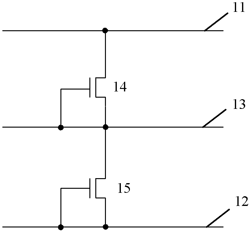
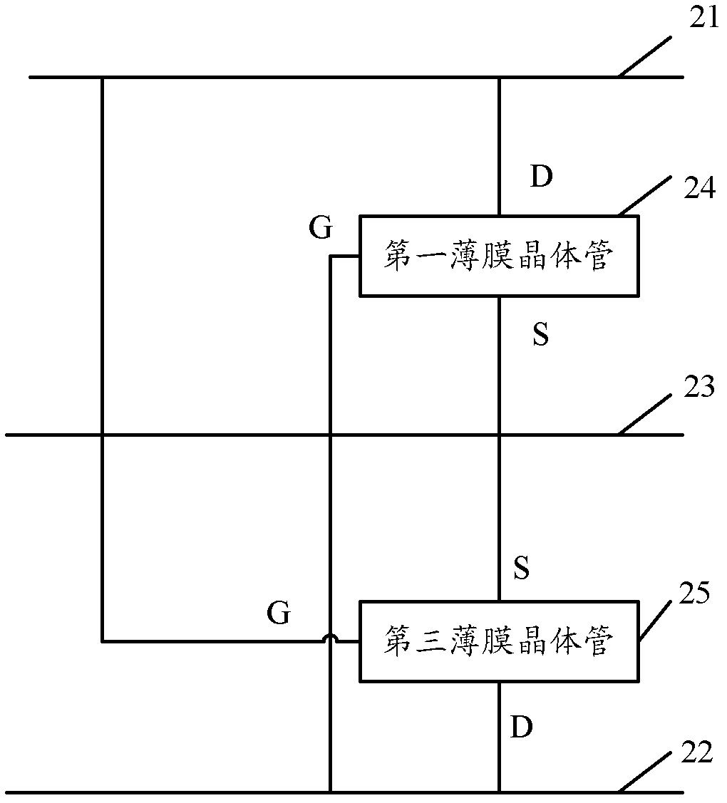
[0015] Such as figure 2 As shown, the circuit in this embodiment includes: a first level line 21 , a second level line 22 , a signal line 23 , a first thin film transistor 24 and a second thin film transistor 25 .

[0016] The gate of the first thin film transistor 24 is connected to the second level line 22, the drain is connected to the first level line 21, and the source is connected to the signal line 23; the gate of the second thin film transistor 25 is connected to the first level line 21, the drain is connected to the second level line 22, and the source is connected to the signal line 23. According to the structural characteristics of the thin ...


PUM


Abstract

The invention discloses a static discharge protective circuit and a display device comprising the static discharge protective circuit. The static discharge protective circuit comprises a first thin film transistor and a second thin film transistor which are depletion type thin film transistors; the gate electrode of the first thin film transistor is connected with a second electrical level wire, the drain electrode of the first thin film transistor is connected with a first electrical level wire, and the source electrode of the first thin film transistor is connected with a signal wire; and the gate electrode of the second thin film transistor is connected with the first electrical level wire, the drain electrode of the second thin film transistor is connected with the second electrical level wire, and the source electrode of the second thin film transistor is connected with the signal wire. In normal operation state, the static discharge protective circuit can effectively prevent thesignal wire from discharging a large amount of current and ensure internal arrays in the display device to operate normally; and when static electricity is generated, the static charges accumulated in the signal wire can be quickly released, and the internal arrays in the display device are protected from static damage. According to the static discharge protective circuit and the display device, the depletion type thin film transistors with low cost are adopted to realize static discharge, the production cost of the static discharge protective circuit is reduced, and the production cost of the display device comprising the static discharge protective circuit is accordingly reduced.

Description

technical field [0001] The invention relates to the field of display technology, in particular to an electrostatic discharge protection circuit and a display device including the circuit. Background technique [0002] ESD (Electro-Static Discharge, electrostatic discharge) protection circuit is on the TFT LCD (Thin Film Transistor Liquid Crystal Display, thin film transistor liquid crystal panel) and AMOLED (Active Matrix Organic Light Emitting Diode, active matrix organic light emitting diode) panel An important part, it can protect display devices from electrostatic damage during production, transportation, and work. [0003] Such as figure 1 A conventional ESD protection circuit shown is composed of two diode-connected P-channel enhanced TFT14 and TFT15. The gate of TFT14 is connected to the signal line 13, the source is connected to the signal line 13, and the drain is connected to the high level line 11; the gate of TFT15 is connected to the low level line 12, and the...

Claims


Application Information

Patent Timeline
IPC IPC(8): H01L27/02G09G3/32
CPCH01L27/0266G09G3/20G09G2330/02G09G2330/04
Inventor 段立业吴仲远袁广才
Owner BOE TECH GRP CO LTD
Why Eureka
Try Eureka