Texturing device and method for silicon solar cells
A technology of silicon solar cells and solar cells, which is applied in the direction of chemical instruments and methods, circuits, electrical components, etc., can solve the problems of reducing the surface reflectivity of silicon solar cells, reducing the damage rate of silicon chips, and shortage of water resources, etc., to achieve Effects of improving photoelectric conversion efficiency, reducing reflectivity, and reducing damage rate
- Summary
- Abstract
- Description
- Claims
- Application Information
AI Technical Summary
Problems solved by technology
Method used
Image

Examples
Embodiment 1
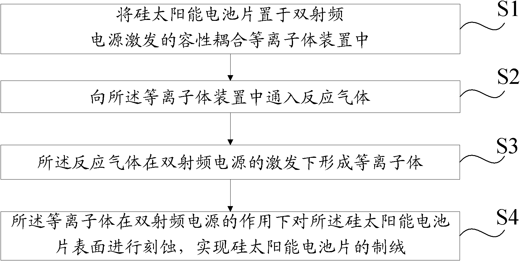
[0041] As mentioned in the background technology section, wet chemical etching is often used in the industry to texture the silicon solar cells (wet texturing for short), and wet texturing needs to consume a large amount of acid and alkali, so there are The problem of shortage of water resources, and the large amount of chemical waste liquid remaining after wet texturing will become one of the sources of environmental pollution. In addition, since the current silicon wafers are becoming thinner and thinner, the silicon wafers treated with acid and alkali solutions are easily broken, resulting in the scrapping of silicon solar cells. Furthermore, the surface reflectance of the obtained silicon solar cells after wet texturing is relatively high, generally more than 23%, and it is difficult to further reduce the reflectivity. Therefore, the photoelectric conversion efficiency of the silicon solar cells cannot be improved.
[0042] Based on this, the present invention provides a m...
Embodiment 2
[0060] In this embodiment, texturing of monocrystalline silicon solar cells is taken as an example for illustration.
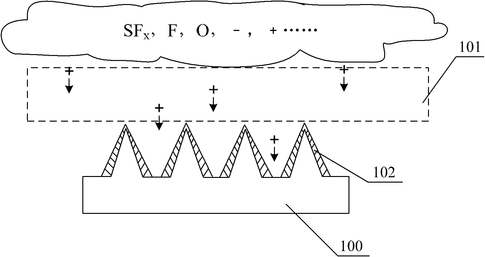
[0061] The single crystal silicon is Czochralski single crystal silicon with n-type (100) crystal plane. The single crystal silicon is placed on the lower electrode in a capacitively coupled plasma device excited by dual radio frequency power sources. The lower electrode can be connected to a water cooling system for cooling, therefore, the lower electrode can also be called a water-cooled substrate holder. Vacuumize the reaction chamber in the plasma device, generally to 5×10 -3 About Pa gets final product, at this moment, lead into SF with the flow rate of 45 sccm by the gas inlet of described plasma device side wall 6 and pass O at a flow rate of 5 sccm 2 , after the gas introduced is stable, adjust the high valve to keep the pressure of the reaction chamber at about 0.75Pa. Then open the upper electrode RF power supply connected to the upper electrode,...
Embodiment 3
[0064] In this embodiment, texturing of monocrystalline silicon solar cells is still taken as an example for illustration.
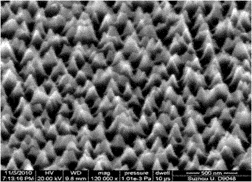
[0065] The difference from Embodiment 2 is that in this embodiment, the power of the upper electrode RF power supply is set to 500W, and other conditions and steps are the same as in Embodiment 2. Finally, after texturing the monocrystalline silicon solar cells After testing, the reflectance of the textured surface of the silicon wafer obtained is 2% at the wavelength of 800 nm. Compared with Example 2, the reflectance of the surface of the silicon solar cell is further reduced. This is due to: increasing the power of the RF power supply of the upper electrode can make the density of the plasma generated in the reaction chamber larger. Therefore, when other conditions are the same, the surface etching of crystalline silicon is carried out more fully, and the texture effect is improved. Better, so as to reduce the reflectivity of the textured surface of t...
PUM
| Property | Measurement | Unit |
|---|---|---|
| power | aaaaa | aaaaa |
| power | aaaaa | aaaaa |
| reflectance | aaaaa | aaaaa |
Abstract
Description
Claims
Application Information
 - R&D Engineer
- R&D Manager
- IP Professional
- Industry Leading Data Capabilities
- Powerful AI technology
- Patent DNA Extraction
Browse by: Latest US Patents, China's latest patents, Technical Efficacy Thesaurus, Application Domain, Technology Topic.
© 2024 PatSnap. All rights reserved.Legal|Privacy policy|Modern Slavery Act Transparency Statement|Sitemap