Attachment for substrates having different diameters, substrate processing apparatus, and method of manufacturing substrate or semiconductor device

A technology for substrate processing devices and accessories, applied in semiconductor/solid-state device manufacturing, electrical components, circuits, etc.

Inactive Publication Date: 2012-09-05
KOKUSA ELECTRIC CO LTD
View PDF4 Cites 6 Cited by
  • Summary
  • Abstract
  • Description
  • Claims
  • Application Information

AI Technical Summary

Problems solved by technology

In addition, it is not limited to a substrate processing apparatus that mixes two kinds of reaction gases inside a reaction chamber to perform SiC epitaxial film formation as in the substrate processing apparatus described in Patent Document 1 above. The same problem occurs in the case of generalization as above

Method used


Image

  • Attachment for substrates having different diameters, substrate processing apparatus, and method of manufacturing substrate or semiconductor device
  • Attachment for substrates having different diameters, substrate processing apparatus, and method of manufacturing substrate or semiconductor device
  • Attachment for substrates having different diameters, substrate processing apparatus, and method of manufacturing substrate or semiconductor device

Examples


no. 1 approach

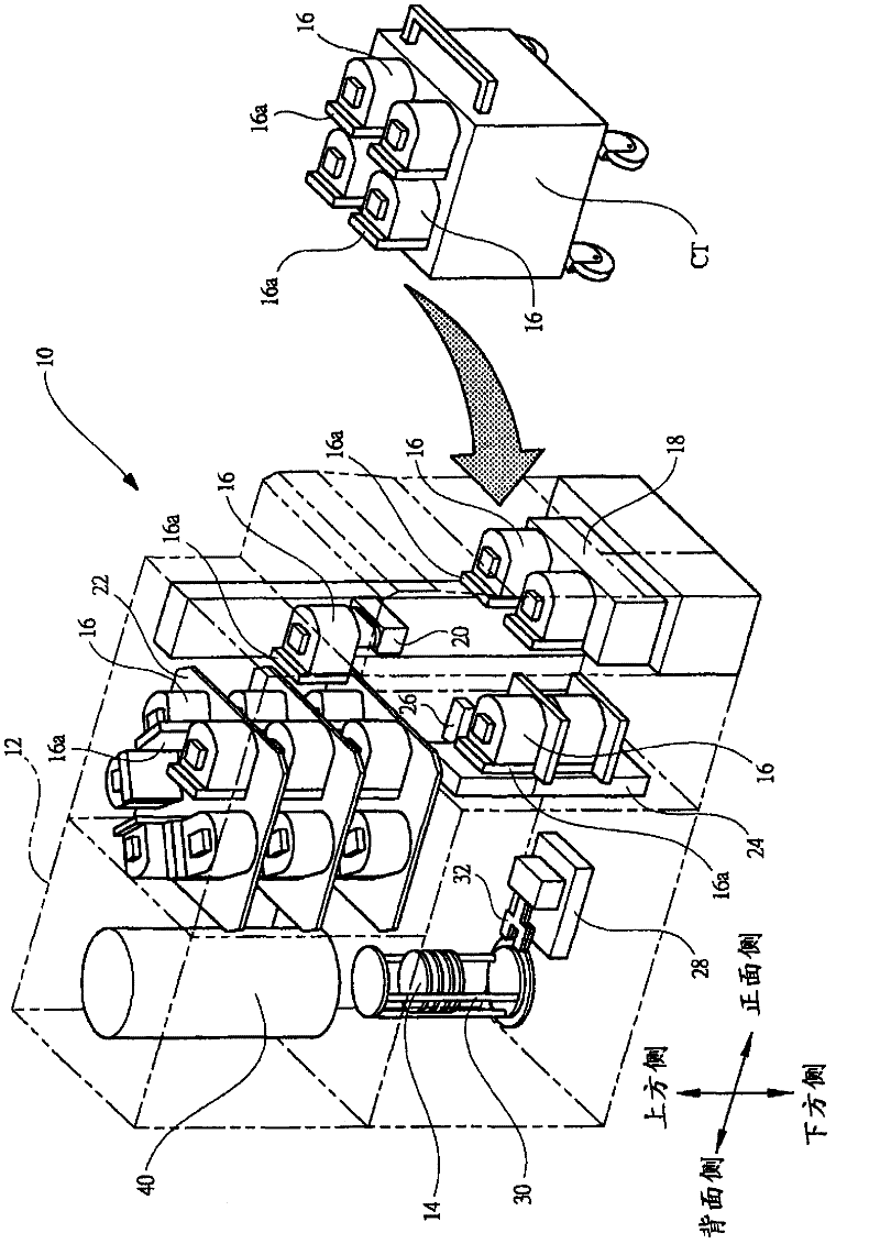
[0037] Next, a first embodiment of the present invention will be described in detail with reference to the drawings. In the following embodiments, a so-called batch-type vertical SiC epitaxial growth device that stacks SiC wafers in the height direction (vertical direction) is exemplified as a SiC epitaxial growth device that is an example of a substrate processing device. Thus, productivity (manufacturing efficiency) is improved by increasing the number of SiC wafers that can be processed at one time.

[0038]

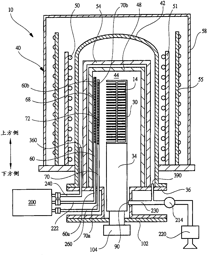
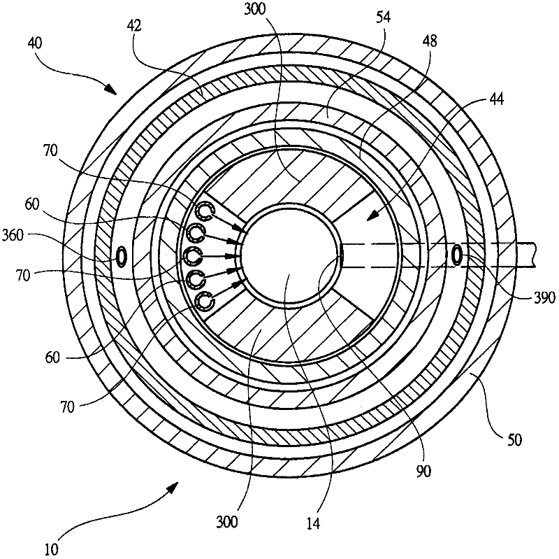
[0039] figure 1 It is a perspective view showing the outline of a substrate processing apparatus using the attachment for substrates with different diameters of the present invention. First, use figure 1 A substrate processing apparatus for forming an SiC epitaxial film and a substrate manufacturing method for forming an SiC epitaxial film as one of the manufacturing steps of a semiconductor device according to an embodiment of the present invention will be describ...

no. 2 approach

[0155] Next, a second embodiment of the present invention will be described in detail with reference to the drawings. In addition, the same code|symbol is attached|subjected to the part which has the same function as 1st Embodiment mentioned above, and the detailed description is abbreviate|omitted.

[0156] Figure 14 (a), (b) and Figure 13 The corresponding figure is shown.

[0157] like Figure 14 As shown in (a), the difference of the attachment 500 for substrates with different diameters according to the second embodiment is that the wafer holder 100 on which the wafer 14 is mounted is shifted (eccentrically) by a distance L toward the side portion 16b of the wafer cassette 16. . That is, the center position of wafer 14 is located on the cover 16a side of wafer cassette 16 compared to the center position of an 8-inch wafer assuming that an 8-inch (first size) wafer is supported in first support groove 16e. Along with this, the second pressing unit 410 is omitted fro...

no. 3 approach

[0163] Next, a third embodiment of the present invention will be described in detail with reference to the drawings. In addition, the same code|symbol is attached|subjected to the part which has the same function as each above-mentioned embodiment, and the detailed description is abbreviate|omitted.

[0164] Figure 15 shows the structure of the attachment for substrates with different diameters according to the third embodiment, and Figure 10 corresponding figure, Figure 16 is enlarged Figure 15 An enlarged cross-sectional view of part B of the dotted circle, Figure 17 (a) and (b) are instructions Figure 15 An explanatory diagram of the operation device of the attachment for substrates with different diameters.

[0165] Such as Figure 15 As shown, the attachment 600 for substrates with different diameters according to the third embodiment has a plate-shaped member 601 supported in each of the first support grooves 16 e provided in the wafer cassette 16 . Each pla...


PUM


Abstract

A downsized substrate may be housed in a substrate accommodation vessel (FOUP) constituting a transfer system corresponding to a large diameter substrate. An attachment includes an upper plate and a lower plate supported by a first support groove that can support an 8-inch wafer, and holding columns installed at the upper plate and the lower plate and including a second support groove that can support a 2-inch wafer (if necessary, via a wafer holder and a holder member). Accordingly, the 2-inch wafer can be housed in a pod corresponding to the 8-inch wafer, and the pod, which is a transfer system, can be standardized to reduce cost of a semiconductor manufacturing apparatus. In addition, a distance from each gas supply nozzle to the wafer can be increased to sufficiently mix reactive gases before arrival at the wafer and improve film-forming precision to the wafer.

Description

technical field [0001] The present invention relates to an accessory for substrates with different diameters, a substrate processing apparatus, and a method for manufacturing substrates or semiconductor devices. different substrates. Background technique [0002] Silicon carbide (SiC) is attracting attention especially as an element material for power devices because it has higher dielectric strength and thermal conductivity than silicon (Si). On the other hand, it is known that SiC is not easy to manufacture crystal substrates and semiconductor devices (semiconductor devices) compared to Si because of the lower diffusion coefficient of impurities. For example, the epitaxial film formation temperature of SiC is about 1500°C to 1800°C compared to the epitaxial film formation temperature of Si, which is about 900°C to 1200°C. effort. As a substrate processing apparatus for performing such SiC epitaxial film formation, for example, the technique described in Patent Document ...

Claims


Application Information

Patent Timeline
Patent Type & Authority Applications(China)
IPC IPC(8): H01L21/673H01L21/205
CPCH01L21/67303H01L21/67309H01L21/67724H01L21/67757
Inventor 伊藤刚田中昭典
Owner KOKUSA ELECTRIC CO LTD
Why Eureka
Try Eureka