Unlock instant, AI-driven research and patent intelligence for your innovation.

TFT (thin film transistor) array substrate, manufacturing method for same, and liquid crystal displayer

A technology for array substrates and substrates, which is used in semiconductor/solid-state device manufacturing, instruments, electrical solid-state devices, etc., and can solve the problem that the bonding drive signal in the pad area cannot be transmitted to the display area of ​​the substrate.

Active Publication Date: 2012-09-05
BEIJING BOE OPTOELECTRONCIS TECH CO LTD
View PDF2 Cites 4 Cited by
  • Summary
  • Abstract
  • Description
  • Claims
  • Application Information

AI Technical Summary

Problems solved by technology

[0004] Embodiments of the present invention provide a TFT array substrate, an access method, and a liquid crystal display, which solve the problem that the driving signal cannot be transmitted to the display area of ​​the substrate due to corrosion or poor adhesion in the pad area to a certain extent.

Method used


Image

  • TFT (thin film transistor) array substrate, manufacturing method for same, and liquid crystal displayer
  • TFT (thin film transistor) array substrate, manufacturing method for same, and liquid crystal displayer
  • TFT (thin film transistor) array substrate, manufacturing method for same, and liquid crystal displayer

Examples


Embodiment Construction

[0040] The following will clearly and completely describe the technical solutions in the embodiments of the present invention with reference to the drawings in the embodiments of the present invention. Apparently, the described embodiments are only some of the embodiments of the present invention, but not all of them. Based on the embodiments of the present invention, all other embodiments obtained by persons of ordinary skill in the art without making creative efforts belong to the protection scope of the present invention.

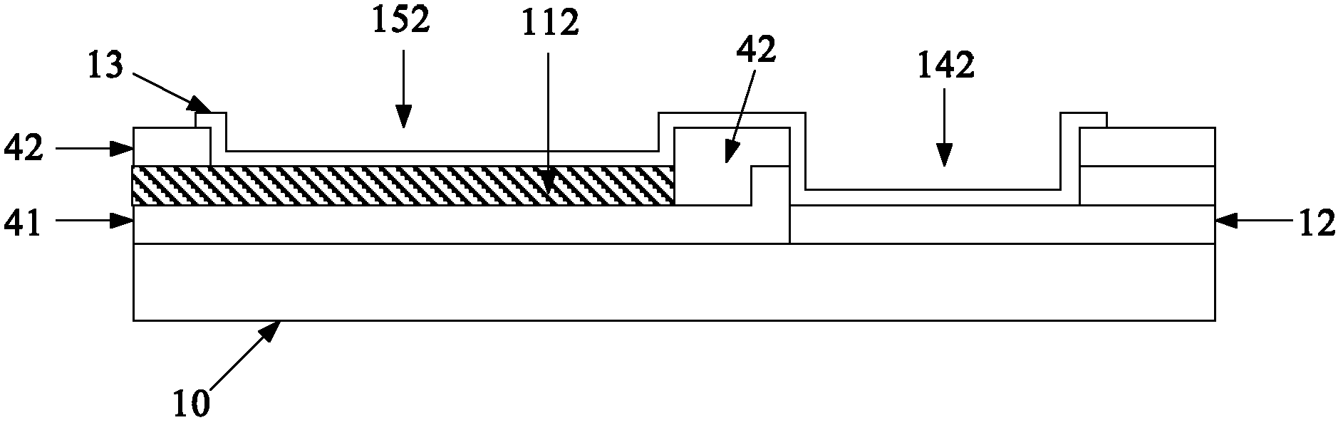
[0041] In each of the following embodiments, the reference numerals of the same parts are marked only in one place, and the rest of the same parts are not marked, but the reference numerals of the marked parts are applicable.

[0042] The TFT array substrate provided by the embodiment of the present invention sequentially includes a gate line layer, a first insulating layer, a semiconductor active layer, a data line layer, a second insulating layer and a...


PUM


Abstract

The embodiment of the invention provides a TFT (thin film transistor) array substrate, a manufacturing method for the same, and a liquid crystal displayer, relating to the field of manufacturing for liquid crystal displayer, and solving the problem that a drive signal cannot be transmitted to a display area of a substrate due to corrosion or bad bonding on a welding pad area. The TFT array substrate sequentially comprises a gate line layer, a first insulating layer, a semiconductor active layer, a data line layer, a second insulating layer, and a transparent conducting layer; and the welding pad area of the TFT array substrate comprises a plurality of leads, wherein each lead is electrically connected with at least two bonding areas. The method provided by the embodiment of the invention is used for manufacturing a TFT substrate.

Description

technical field [0001] The invention relates to the field of manufacturing liquid crystal displays, in particular to a TFT array substrate, a manufacturing method thereof, and a liquid crystal display. Background technique [0002] In the TFT-LCD (Thin Film Transistor-Liquid Crystal Display, Thin Film Field Effect Transistor-Liquid Crystal Display) manufacturing process, the TFT array substrate needs to be bonded with an integrated circuit or a flexible circuit board to transmit the driving signal to the display area of ​​the substrate. [0003] On the bonding pad area where the TFT array substrate is bonded to the integrated circuit or flexible circuit board, the lead wires are prone to corrosion and other phenomena, resulting in poor adhesion, so that the driving signal cannot be effectively transmitted to the display area of ​​the substrate, resulting in poor picture quality. . Contents of the invention [0004] Embodiments of the present invention provide a TFT array ...

Claims


Application Information

Patent Timeline
IPC IPC(8): H01L27/02H01L23/58H01L21/77G02F1/1362G02F1/1368
Inventor 李鑫冯京唐磊
Owner BEIJING BOE OPTOELECTRONCIS TECH CO LTD
Features
  • R&D
  • Intellectual Property
  • Life Sciences
  • Materials
  • Tech Scout
  • Unparalleled Data Quality
  • Higher Quality Content
  • 60% Fewer Hallucinations
Learn More