
Forming method of performing forming on variable resistance nonvolatile memory element, and variable resistance nonvolatile memory device

A non-volatile storage and resistance-variable technology, applied in electrical components, information storage, static memory, etc., can solve the problems of high voltage formed by resistance-variable components, insufficient and low resistance values, etc.

Active Publication Date: 2014-07-23
PANASONIC SEMICON SOLUTIONS CO LTD
View PDF7 Cites 0 Cited by
  • Summary
  • Abstract
  • Description
  • Claims
  • Application Information

AI Technical Summary

Problems solved by technology

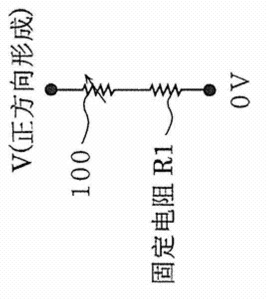
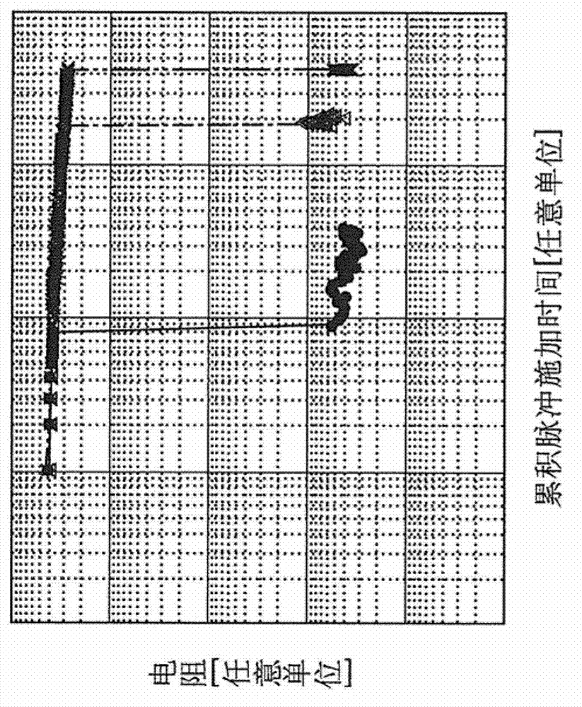
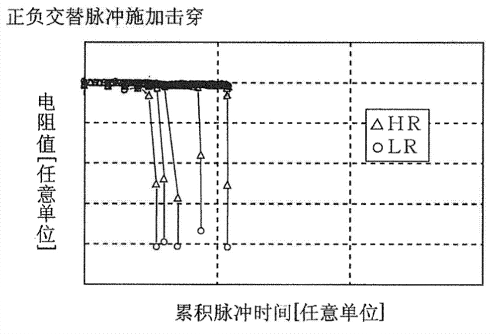
[0045] However, the above-mentioned conventional resistance variable semiconductor memory device has a problem that the formation voltage is not uniform for each resistance variable element constituting the memory cell array, or that the initial voltage applied to the resistance to transition to the state where the resistance change starts is The formation voltage of the change element becomes higher
In addition, although it will be described in detail later, it is clear that there is another problem in the formation method according to the related invention for solving such a problem that the cell current in the low-resistance state decreases (that is, the low resistance of the resistance variable element Insufficient resistance value in the state becomes low)

Method used


Image

  • Forming method of performing forming on variable resistance nonvolatile memory element, and variable resistance nonvolatile memory device
  • Forming method of performing forming on variable resistance nonvolatile memory element, and variable resistance nonvolatile memory device
  • Forming method of performing forming on variable resistance nonvolatile memory element, and variable resistance nonvolatile memory device

Examples


no. 2 Embodiment approach

[0284] Next, the realization will be described Figure 16 An example of a nonvolatile memory device having a flow of the formation of , is taken as the second embodiment of the present invention.

[0285] (Non-volatile memory device according to the second embodiment)

[0286] Figure 19This is a block diagram showing an example of the configuration of a variable resistance nonvolatile memory device 200 (hereinafter simply referred to as a nonvolatile memory device 200 ) according to the second embodiment of the present invention. and, Figure 20 is shown Figure 19 A perspective view of the structure of the A part (the structure of the 4-position part).

[0287] like Figure 19 The nonvolatile memory device 200 according to the present embodiment includes a memory main body portion 201 on a semiconductor substrate, and the memory main body portion 201 includes: a memory cell array 202; a row selection circuit / driver 203; a column selection circuit / driver 204; The writin...

no. 3 Embodiment approach

[0370] Next, the third embodiment of the present invention will describe a case in which the automatic formation control circuit 211 and the automatic formation circuit 210 in the nonvolatile memory device described in the second embodiment are not provided in the device, and from The outside of the nonvolatile memory device is controlled and implemented.

[0371] (Nonvolatile memory device according to the third embodiment)

[0372] Figure 26 It is a block diagram showing an example of the configuration of the variable resistance nonvolatile memory device 400 (hereinafter, simply referred to as the nonvolatile memory device 400 ) according to the embodiment of the present invention.

[0373] like Figure 26 As shown, the nonvolatile memory device 400 according to this embodiment includes a memory main body 401 on a semiconductor substrate, and the memory main body 401 includes a memory cell array 402 for Figure 39 The illustrated upper electrode 100c utilizes 1T1R type m...


PUM


Abstract

When the variable resistance nonvolatile memory element having a first electrode, a second electrode, and a transition metal oxide layer sandwiched between the first electrode and the second electrode is in an initial state, the first electrode A first forming voltage is applied between the first electrode and the second electrode until the first formation of the first operable state reversibly transitioned between the high resistance state and the low resistance state occurs, between the first electrode and the second electrode. Applying a second forming voltage between the second electrodes until it changes to a resistance value lower than the resistance value of the low resistance state in the first operable state after the first formation. Formation of the variable resistance nonvolatile memory element proceeds until the second formation of the second operable state of the resistance state is performed.

Description

technical field [0001] The present invention relates to a formation (initialization) method for stably changing resistance of a resistance variable nonvolatile memory element whose resistance value is reversibly changed in accordance with an electrical signal, and a resistance variable nonvolatile memory having that function device. Background technique [0002] In recent years, resistance variable nonvolatile memory devices (hereinafter also simply referred to as "resistance variable elements") including memory cells constructed using resistance variable nonvolatile memory elements (hereinafter also simply referred to as "resistance variable elements") have been developed. "Non-volatile memory device".) research and development. The variable resistance element refers to an element that has a property of reversibly changing a resistance value according to an electric signal, and can further store data corresponding to the resistance value in a nonvolatile manner. [0003] ...

Claims


Application Information

Patent Timeline
Patent Type & Authority Patents(China)
IPC IPC(8): G11C13/00H01L27/10H01L27/105H01L45/00H01L49/00H10N99/00
CPCG11C2213/32H01L45/146H01L27/2409G11C13/0007G11C2013/0083H01L27/101G11C2213/72H01L45/1233G11C2213/79G11C13/0069H01L45/08G11C2013/0073G11C13/0064H10B63/20H10N70/24H10N70/826H10N70/8833
Inventor 河合贤岛川一彦片山幸治村冈俊作
Owner PANASONIC SEMICON SOLUTIONS CO LTD
Learn More