Supercharge Your Innovation With Domain-Expert AI Agents!

Photoetching simulation method and device

A simulation method and lithography technology, applied in the field of lithography simulation, can solve problems such as slow speed and affect the design efficiency of integrated circuits, and achieve the effect of improving simulation speed and reducing simulation computing tasks.

Active Publication Date: 2012-09-19
INST OF MICROELECTRONICS CHINESE ACAD OF SCI
View PDF5 Cites 6 Cited by
  • Summary
  • Abstract
  • Description
  • Claims
  • Application Information

AI Technical Summary

Problems solved by technology

[0004] In the process of realizing the present invention, the applicant realizes that there are technical problems in the prior art: the traditional serial and parallel lithography simulation needs to make detailed and complex simulation calculations for each tiny area of ​​the integrated circuit layout, so the speed comparison Slow, which affects the improvement of integrated circuit design efficiency

Method used


Image

  • Photoetching simulation method and device
  • Photoetching simulation method and device
  • Photoetching simulation method and device

Examples


Embodiment Construction

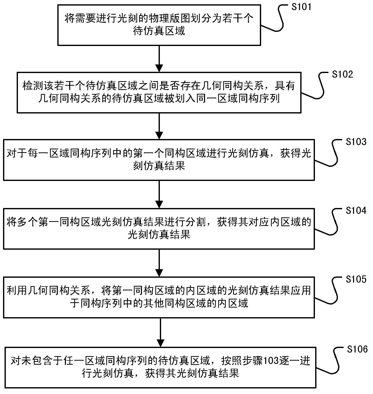
[0020] In order to make the object, technical solution and advantages of the present invention clearer, the present invention will be described in further detail below in conjunction with specific embodiments and with reference to the accompanying drawings. While illustrations of parameters including particular values ​​may be provided herein, it should be understood that parameters need not be exactly equal to the corresponding values, but rather may approximate the values ​​within acceptable error margins or design constraints.

[0021] In the physical design of integrated circuits, there is a great deal of similarity in design patterns between local regions, which determines the similarity of lithography calculation process and calculation results between local regions. Based on the above findings, the present invention merges lithography simulation tasks in a graph isomorphism manner, performs a calculation on the same physical layout lithography simulation task based on gr...


PUM


Abstract

The invention discloses a photoetching simulation method and a photoetching simulation device. The photoetching simulation method comprises the following steps of: dividing a mask figure in a physical domain into a plurality of to-be-simulated regions; searching the to-be-simulated regions with geometric isomorphic relation from the plurality of to-be-simulated regions, wherein the to-be-simulated regions with geometric isomorphic relation and acquired by search are formed into region isomorphic sequences; and combining photoetching simulation tasks for each of the plurality of region isomorphic sequences in a figure isomorphic mode to obtain the photoetching simulation result. In the photoetching simulation method and the photoetching simulation device, complex simulation calculation tasks can be effectively reduced by multiplexing of region photoetching simulation data, and the whole photoetching simulation speed of a chip is increased on the premise of not sacrificing the simulation precision.

Description

technical field [0001] The invention relates to the field of manufacturability design of integrated circuits in the microelectronics industry and the automation of integrated circuit design, in particular to a method and device for lithography simulation. Background technique [0002] Photolithography is an important step in the integrated circuit manufacturing process. As the integrated circuit manufacturing process enters the 65-45nm process node, since the wavelength of light used for exposure is much larger than the size and spacing between the ideal graphics of physical layout design, the light wave The interference and diffraction effects of the actual lithography make there is a big difference between the ideal graphics designed for physical graphics and physical layouts. The shape and spacing of the actual graphics change greatly, and even affect the performance of the circuit. The corresponding physical A design is called a hot spot, which indicates a problem and ne...

Claims


Application Information

Patent Timeline
IPC IPC(8): G03F7/20G06F17/50
Inventor 陈岚李志刚吴玉平
Owner INST OF MICROELECTRONICS CHINESE ACAD OF SCI
Features
  • R&D
  • Intellectual Property
  • Life Sciences
  • Materials
  • Tech Scout
  • Unparalleled Data Quality
  • Higher Quality Content
  • 60% Fewer Hallucinations
Learn More