Transparent conductive film and touch panel

一种透明导电性、透明导电层的技术,应用在绝缘载体上的导电层、电路、电气元件等方向,能够解决薄膜处理性差、透明导电性薄膜卷曲、表面凹凸形成不充分等问题,达到处理性优异、透明性及外观特性优异的效果

Active Publication Date: 2012-09-19
NITTO DENKO CORP
View PDF9 Cites 7 Cited by
  • Summary
  • Abstract
  • Description
  • Claims
  • Application Information

AI Technical Summary

Problems solved by technology

However, according to the studies of the inventors of the present application, it is clear that if the thickness of the cured resin layer formed by using a coating resin composition having two or more components that undergoes phase separation becomes large, the transparent conductive layer will Since the transparent conductive film curls due to heating during crystallization and touch panel formation, it tends to be poor in handling of the film as a problem different from sliding properties and anti-blocking properties
On the other hand, it is clear that if the thickness of the cured resin layer is reduced, the occurrence of curl can be suppressed, but the formation of surface irregularities is insufficient and unevenness occurs in the formation of surface irregularities, so there is a problem that it is difficult to obtain stable resistance. Tendency to stickiness and slipperiness

Method used


Image

  • Transparent conductive film and touch panel
  • Transparent conductive film and touch panel
  • Transparent conductive film and touch panel

Examples


Embodiment 1

[0106] (Preparation of Coating Composition)

[0107] Prepare a resin solution as follows: a resin solution containing a resin composition for forming surface irregularities by phase separation and a resin component including a photopolymerization initiator at a solid content concentration of 60% by weight in a mixed solvent of methyl ethyl ketone and methyl isobutyl ketone (trade name "Lucifral NAB-007" manufactured by Nippon Paint Co., Ltd.).

[0108] Acrylic fine particles (trade name "BMSA-18GN" manufactured by Sekisui Plastics Co., Ltd. (average particle diameter: 0.8 μm)) were dispersed in methyl isobutyl ketone, and the dispersion was mixed with the aforementioned resin solution to prepare A coating composition containing 0.1 part by weight of acrylic fine particles per 100 parts by weight of a resin component and having a solid content concentration of 40% by weight.

[0109] (Formation of cured resin layer)

[0110] Using a bar coater, the aforementioned coating compos...

Embodiment 2

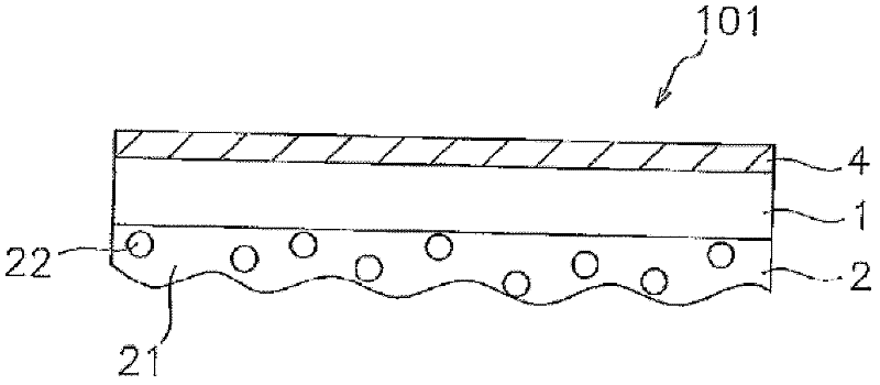
[0115] In Example 1, except that the thickness of the cured resin layer was changed to 2.7 μm, it was formed in the same manner as in Example 1. figure 1 A transparent conductive film in the stacked form shown.

Embodiment 3

[0117] In Example 1, except that the thickness of the cured resin layer was changed to 1.1 μm, the same method as in Example 1 was formed. figure 1 A transparent conductive film in the stacked form shown.


PUM

PropertyMeasurementUnit
particle diameteraaaaaaaaaa
roughnessaaaaaaaaaa
particle diameteraaaaaaaaaa

Abstract

The invention provides a transparent conductive film and a touch panel, the transparent conductive film has a blocking resistance and has a good transparency and an appearance characteristic. The transparent conductive film has a transparent polymer substrate and a transparent conductive layer on one main surface of the transparent polymer substrate. A cured resin layer with surface irregularities is formed: at least one of: between the transparent polymer substrate and the transparent conductive layer; and on the main surface opposite to the surface with the transparent conductive layer formed thereon of the transparent polymer substrate. The cured resin layer is preferably 1 [mu]m or more and 3 [mu]m or less in thickness and preferably contains a resin composition containing at least two components that undergo phase separation based on a difference in physical properties and 0.01 to 5 parts by weight of fine particles to 100 parts by weight of the solid content of the resin composition. The particle size of the fine particles is preferably 25 to 80% of the thickness of the cured resin layer.

Description

technical field [0001] The present invention relates to a transparent conductive film provided with a transparent conductive layer on a film substrate and a manufacturing method thereof. The transparent conductive film of the present invention is suitable for use in touch panel applications. Background technique [0002] A transparent conductive film formed by forming a transparent conductive film on a transparent polymer substrate is widely used in solar cells, transparent electrodes for inorganic EL elements, organic EL elements, electromagnetic wave shielding materials, touch panels, and the like. In particular, in recent years, the mounting rate of touch panels in mobile phones, portable game machines, and the like has increased, and the demand for transparent conductive films has rapidly expanded. [0003] Widely used as transparent conductive films for touch panels and the like. Conductive metal oxide films such as indium-tin composite oxide (ITO) are formed on flexib...

Claims


Application Information

Patent Timeline
Patent Type & Authority Applications(China)
IPC IPC(8): H01B5/14H01B13/00G06F3/041B32B3/30B32B27/04C08J7/043C08J7/044C08J7/046
CPCH01B13/00G06F3/041H01B5/14B32B27/04B32B3/30C08J2367/02C08J2433/00Y10T428/24405C08J7/0423C08J7/0427C08J7/043C08J7/046C08J7/044G02F1/13338
Inventor 小泽博纪鹰尾宽行金谷实长竹涉
Owner NITTO DENKO CORP
Why Eureka
Try Eureka