Inverted type transparent organic electroluminescent device and preparation method thereof
A luminescent and inverted technology, applied in the field of electric light sources, can solve the problems of limiting the application range of OLEDs, low luminous intensity, and concentration of unfavorable light, so as to improve lifespan and luminous stability, broaden the application range, and improve luminous performance effect
- Summary
- Abstract
- Description
- Claims
- Application Information
AI Technical Summary
Problems solved by technology
Method used
Image
Examples
preparation example Construction
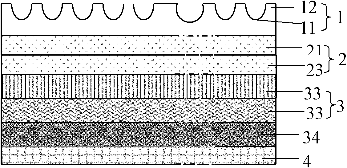
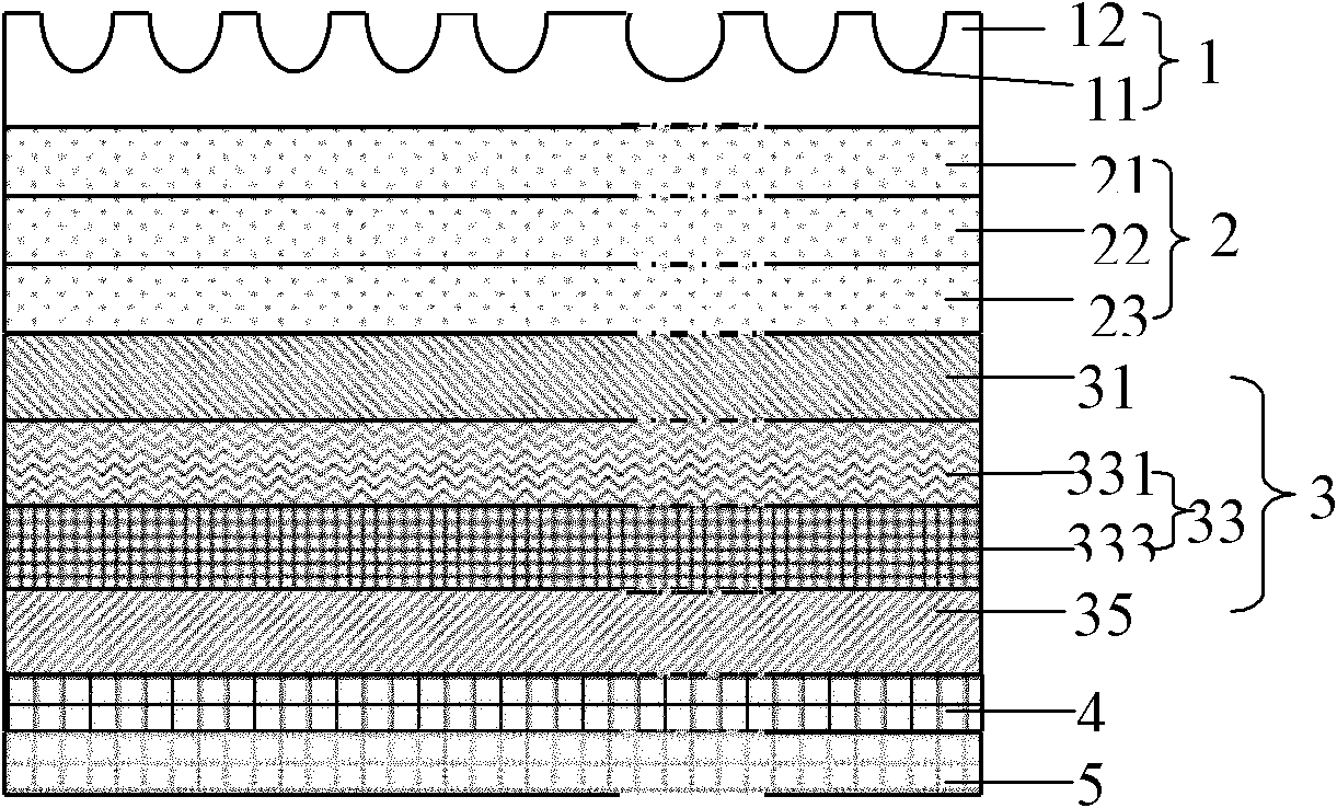
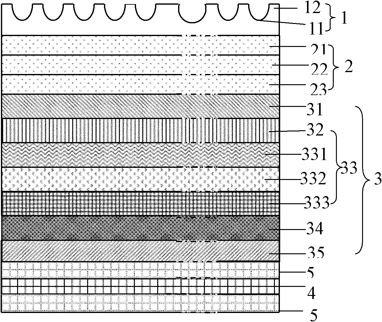
[0041] The embodiment of the present invention also provides a method for preparing the above-mentioned inverted transparent organic electroluminescent device, the process flow chart of the method is as follows Figure 4 shown, see also figure 1 or figure 2 or image 3 , the method includes the following steps:
[0042] S1. Provide a transparent substrate with an opposite first surface and a second surface, and form an array-distributed concave lens 11-type concave portion on the first surface of the transparent substrate to prepare a transparent substrate 1; wherein, the first surface of the transparent substrate Constituting the first surface of the light-transmitting substrate 1, the second surface of the transparent substrate is the second surface of the light-transmitting substrate 1;
[0043] S2. Plating a transparent cathode 2 on the second surface of the transparent substrate 1;
[0044] S3. Coating an organic electroluminescent structure 3 on the surface of the t...
Embodiment 1
[0055] The structure of the inverted transparent organic electroluminescence device of this embodiment is as follows figure 1 As shown, the inverted transparent organic electroluminescent device includes a transparent substrate 1 , a conductive layer 21 , an Al layer 23 , an electron transport layer 32 , a light emitting layer 33 , a hole transport layer 34 and a transparent anode 4 sequentially combined. Wherein, the transparent substrate 1 has opposite first surface and second surface, the first surface has a concave portion of concave lens type 11, the concave portion has a concave surface 12, the second surface is combined with the transparent anode 2, the second surface is a plane, concave lens 11 are distributed in an array on the first surface, the diameter of the concave lens 11 is 20 μm, and the focal length is 30 μm; the conductive layer 21 and the Al layer 23 constitute the transparent cathode 2; the electron transport layer 32, the light-emitting layer 33 and the ho...
Embodiment 2
[0063] The structure of the inverted transparent organic electroluminescence device of this embodiment is as follows figure 2 As shown, the inverted transparent organic electroluminescent device includes a transparent substrate 1, a conductive layer 21, an Ag layer 22, an Al layer 23, an electron injection layer 31, a red light emitting layer 331, a blue light emitting layer 333, and a hole injection layer 35 , transparent anode 4 and anti-reflection film layer 5 . Wherein, the transparent substrate 1 has opposite first surface and second surface, the first surface has a concave portion of concave lens type 11, the concave portion has a concave surface 12, the second surface is combined with the transparent anode 2, the second surface is a plane, concave lens 11 are distributed in an array on the first surface, the diameter of the concave lens 11 is 10 μm, and the focal length is 20 μm; the conductive layer 21, the Ag layer 22, and the Al layer 23 constitute the transparent c...
PUM
 Abstract
Description
Claims
Application Information


