

Silk-screen printing method for positive electrode of solar battery
A technology of solar cells and screen printing, applied in printing, circuits, printing devices, etc., can solve the problems of the decline of the electrical properties of silicon wafers, the decline of the electrical properties of the silicon wafers to be printed, and the overall performance of the silicon wafers to be printed. The effect of degrading electrical performance and improving overall performance
- Summary
- Abstract
- Description
- Claims
- Application Information
AI Technical Summary
Problems solved by technology
Method used
Image

Examples
Embodiment Construction
[0022] In order to make the purpose, technical solutions and advantages of the embodiments of the present invention clearer, the technical solutions in the embodiments of the present invention will be clearly and completely described below in conjunction with the drawings in the embodiments of the present invention. Obviously, the described embodiments It is a part of embodiments of the present invention, but not all embodiments. Based on the embodiments of the present invention, all other embodiments obtained by persons of ordinary skill in the art without making creative efforts belong to the protection scope of the present invention.
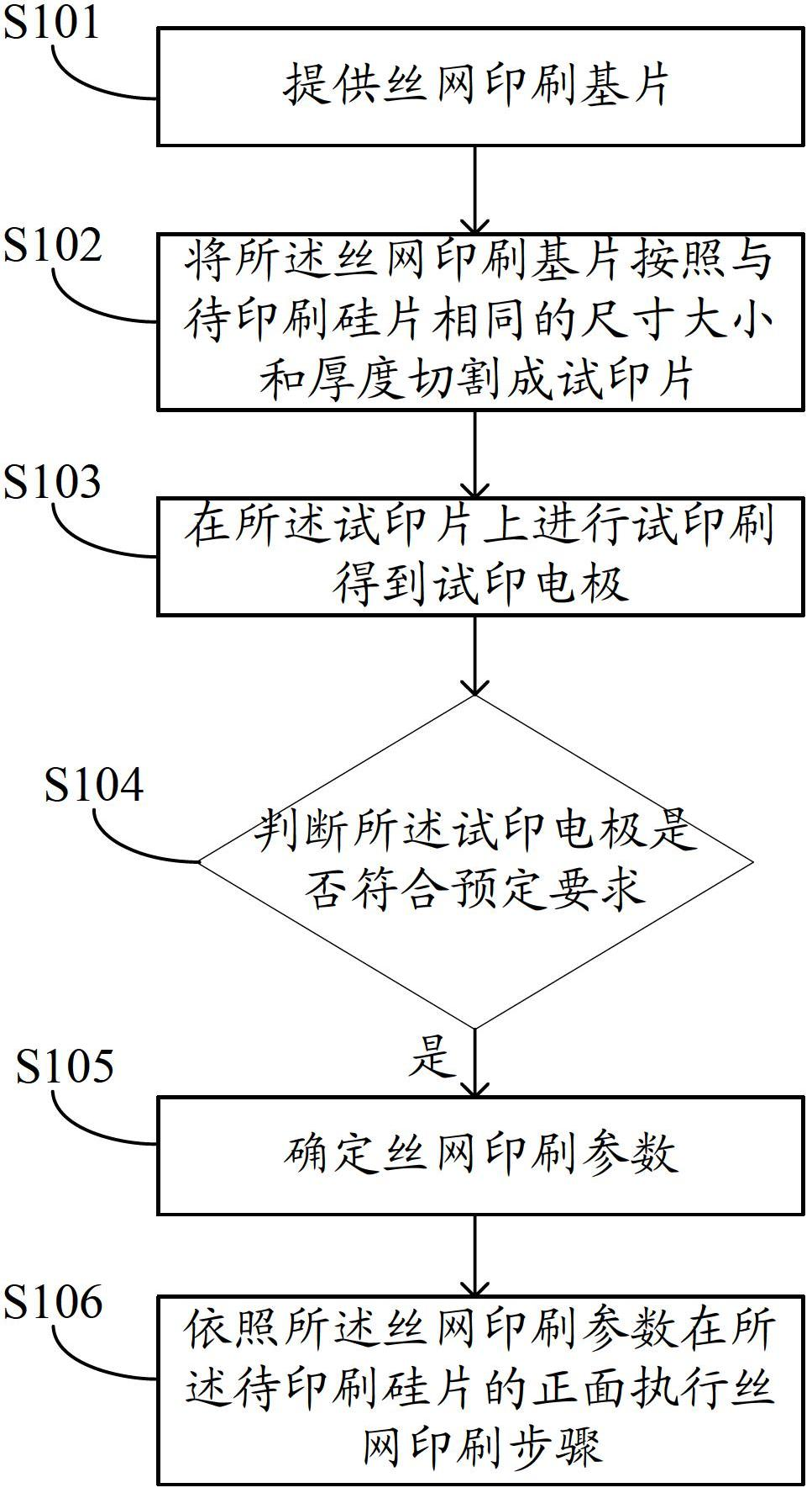
[0023] In order to avoid the degradation of the overall performance of the silicon wafer after the front electrode is finally formed on the silicon wafer due to the trial printing process of the silicon wafer, an embodiment of the present invention provides a screen printing method for the front electrode of a solar cell. figure 1 A flowchart...
PUM
 Abstract
Description
Claims
Application Information