Circuit device of graphene transistor and preparation method thereof

A circuit device and transistor technology, which is applied in the manufacture of transistors, circuits, semiconductors/solid-state devices, etc., can solve problems such as lack of molding and complexity, and achieve the effect of avoiding the reduction of electrical performance

Pending Publication Date: 2018-12-11
UNIV OF SCI & TECH OF CHINA
View PDF0 Cites 0 Cited by
  • Summary
  • Abstract
  • Description
  • Claims
  • Application Information

AI Technical Summary

Problems solved by technology

[0004] In addition, large-scale integrated circuits are still based on silicon-based semiconductors, and the tape-out process of silicon-based semiconductors is very complicated. From the processing of raw mate

Method used


Image

  • Circuit device of graphene transistor and preparation method thereof
  • Circuit device of graphene transistor and preparation method thereof
  • Circuit device of graphene transistor and preparation method thereof

Examples


Embodiment 1

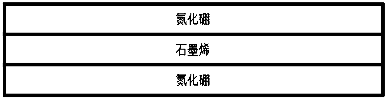
[0053] A boron nitride / graphene / boron nitride heterojunction is provided: in a CVD facility (available from Shenyang Keyi), boron is utilized on a 25 micron thick copper foil (available from CALCO) using a CVD method The precursor (available from Gelest, USA) grows a layer of boron nitride, the growth temperature is 1035 ° C, the growth time is 20 minutes, the boron precursor used is boron azine (available from Gelest, USA), by the carrier gas bubbling method It is brought into a high temperature region for growth, the carrier gas is argon or nitrogen, and the flow rate of the carrier gas is 0.5 sccm to obtain a boron nitride layer (0.3 nanometer thickness) on the copper foil. After the growth of the first layer of boron nitride was completed, nitrogen was introduced for purging for 30s. Then a 25-micron thick copper foil catalyst was placed 50 microns above the growth base copper foil, and methane (available from Linde gas) was introduced to start growing a graphene layer as ...

Embodiment 2

[0058] This embodiment provides another second electrode layer or even more electrode layers in order to realize some more complex functions on the graphene transistor circuit device (having one electrode layer) obtained in the above-mentioned embodiment 1. In order to provide an additional second electrode layer or more electrode layers, an oxide insulating layer needs to be grown between these electrode layers.

[0059] Specifically, on the graphene transistor circuit device obtained in Example 1, a 50 nm-thick aluminum oxide layer was grown on the electrode layer by the ALD method to serve as an oxide insulating layer. In the formed oxide insulating layer, five through holes were formed. After that, a second electrode layer is formed on the oxide insulating layer by the same process as in Embodiment 1 for forming the source, drain and gate electrode structures. Due to the existence of the oxide insulating layer, the second electrode layer will not be in direct contact with...

Embodiment 3

[0061] The same procedure as described in Example 1 obtained boron nitride / graphene / boron nitride heterojunctions grown on copper foil.

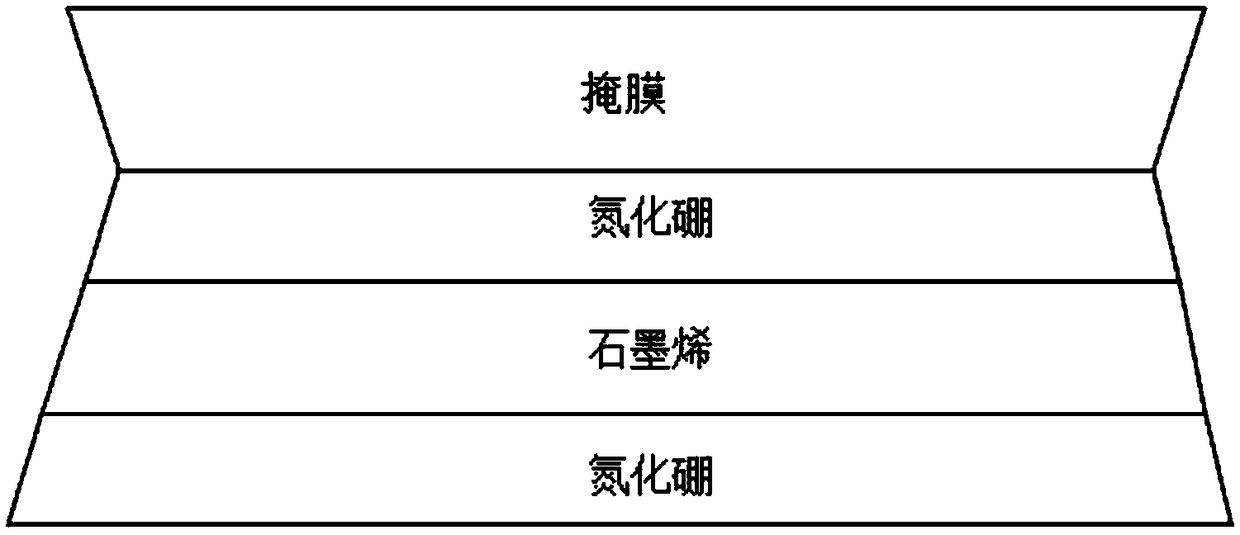
[0062] A layer of PMMA protective glue was spin-coated on the boron nitride / graphene / boron nitride heterojunction grown on the copper foil, the spin-coating speed was 3000 rpm, and the spin-coating time was 2 minutes. After spin coating, bake (KW-4AH-600), the baking temperature is 180℃, and the time is 5 minutes. The baked samples (ie, copper foil / heterojunction / PMMA layer) were horizontally placed in a 0.25 mol / L ammonium persulfate aqueous solution (purchased from Shanghai Shanghai Style) for 3 hours to etch away the copper foil. . After the copper foil is thoroughly etched, the combination of the PMMA layer and the heterojunction (ie, a thin film) will float on the surface of the aqueous solution. The film was pulled out with a PET sheet (purchased from Hefei Kejing) as the base, and the film and the base were attached. Let stand for ...


PUM

PropertyMeasurementUnit
Thicknessaaaaaaaaaa

Abstract

A graphene transistor circuit device is prepared by providing a boron nitride/graphene/boron nitride heterojunction on a metal substrate and transferring the heterojunction to a desired substrate; Forming a desired transistor structure via a mask and by dry etching; An electrode layer including a source electrode, a drain electrode, and a gate electrode is formed on the heterojunction via an electron beam glue layer. The invention utilizes the boron nitride/graphene/boron nitride heterojunction to not only open the energy gap of the graphene, Moreover, the electrode layer is formed directly onthe boron nitride by vapor deposition, thereby protecting the graphene and avoiding the degradation of the electrical performance caused by the adsorption of gas molecules due to the exposure of thegraphene to the atmospheric environment. Therefore, the invention can utilize the electrical performance of the graphene to prepare a transistor circuit device with excellent performance.

Description

technical field [0001] The invention relates to the field of semiconductor design and manufacture, in particular to a graphene transistor circuit device and a preparation method thereof. Background technique [0002] Since its discovery, graphene has received extensive attention due to its ultra-high electrical properties, but its application in the semiconductor field is limited due to its zero band gap. Therefore, many scientific researchers have begun to work on opening the band gap of graphene to make graphene a semiconductor. At present, there are several ways to open the energy band of graphene, such as forming a heterojunction substrate to induce the opening of the energy gap, chemical doping, hybridization, and bilayer graphene. However, many current methods will destroy the lattice structure of graphene itself, so its electrical properties will be greatly affected. [0003] For example, the applicant provides a FinFET device and a method of manufacturing the same ...

Claims


Application Information

Patent Timeline
IPC IPC(8): H01L21/8234H01L27/088
CPCH01L21/823412H01L27/088
Inventor 郭国平杨晖李海欧曹刚郭光灿
Owner UNIV OF SCI & TECH OF CHINA
Why Eureka
Try Eureka