Chip stacking and packaging structure

A packaging structure and chip stacking technology, which is applied in printed circuit manufacturing, circuits, and electrical solid devices, etc., can solve the problems of low chip heat dissipation, affect chip performance, and low thermal conductivity, and achieve improved electrical performance, shortened length, and high efficiency. cooling effect

Active Publication Date: 2014-12-03
HUAWEI TECH CO LTD
View PDF4 Cites 0 Cited by
  • Summary
  • Abstract
  • Description
  • Claims
  • Application Information

AI Technical Summary

Problems solved by technology

[0003] In the chip stack package structure in the prior art, since the chips are closely stacked together, this stacking method makes the heat dissipation performance of the chips very low
The heat generated by the chip can only be conducted outward through the metal traces and the chip body material, the heat conduction efficiency is very low, and because the high-power chip and the low-power chip are stacked together, the temperature of the low-power chip will rise under the influence of the high-power chip High, which in turn affects chip performance

Method used


Image

  • Chip stacking and packaging structure
  • Chip stacking and packaging structure
  • Chip stacking and packaging structure

Examples


Embodiment Construction

[0023] The following will clearly and completely describe the technical solutions in the embodiments of the present invention with reference to the accompanying drawings in the embodiments of the present invention. Obviously, the described embodiments are only some, not all, embodiments of the present invention. Based on the embodiments of the present invention, all other embodiments obtained by persons of ordinary skill in the art without creative efforts fall within the protection scope of the present invention.

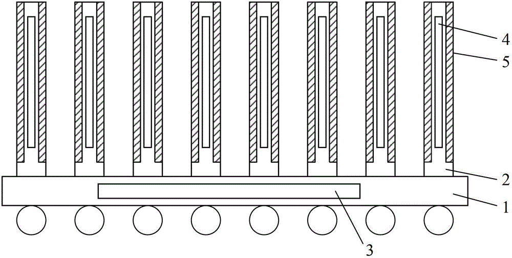
[0024] An embodiment of the present invention provides a chip stack package structure, such as figure 1 As shown, the structure includes:

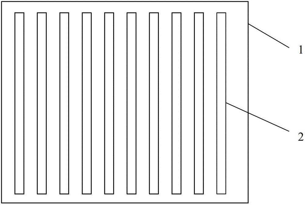
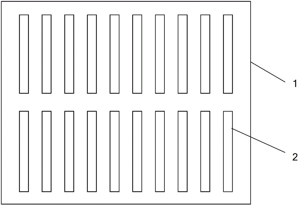
[0025] A main substrate 1 and at least one superimposed substrate 2, the main substrate 1 is provided with a main chip 3, and the superposed substrate 2 is provided with at least one superimposed chip 4;

[0026] The side of the stacked substrate 2 is disposed on the main substrate 1 , so that the stacked chip 4 is connected t...


PUM


Abstract

A chip stack structure, comprising a main substrate (1) and at least one superposed substrate (2). The main substrate (1) is provided therein with a main chip (3). The superposed substrate (2) is provided thereon with at least one superposed chip (4). The sides of the superposed substrate (2) are provided on the main substrate (1), so that the superposed chip (4) is connected to the main chip, realizing a high density stack of chips and improving the heat dissipation efficiency of the chip stack encapsulation structure.

Description

technical field [0001] The invention relates to the technical field of chip packaging, in particular to a chip stack packaging structure. Background technique [0002] In order to meet the requirements of high-density miniaturization of integrated circuits, chip stacking has become a development trend of integrated circuits. In the prior art, the chips are generally stacked in the following way: the chips are placed horizontally and stacked vertically layer by layer. Chips can be connected by laser drilling, that is, laser drilling is performed on the stacked chips, and then the connection between chips is realized by electroplating. [0003] In the stacked chip package structure in the prior art, since the chips are closely stacked horizontally, the stacking method makes the heat dissipation performance of the chips very low. The heat generated by the chip can only be conducted outward through the metal traces and the chip body material, the heat conduction efficiency is ...

Claims


Application Information

Patent Timeline
Patent Type & Authority Patents(China)
IPC IPC(8): H01L25/065H01L23/367H01L23/488
CPCH01L25/10H01L2224/16227H01L2224/73267H01L2225/1035H01L24/20H01L23/367H01L25/0652H01L2224/12105H01L23/5389H05K1/185H05K3/4697H01L23/3736H01L2224/16225H01L2924/12042H01L24/19H01L2224/04105H01L2224/32225H01L2924/15311H01L2225/1064H01L2225/1094H01L2924/00H01L23/34H01L25/18
Inventor 刘伟锋
Owner HUAWEI TECH CO LTD
Why Eureka
Try Eureka