
Laminated ceramic capacitor

A technology of ceramic capacitors and laminates, applied in the direction of multilayer capacitors, capacitors, fixed capacitors, etc., can solve the problem that capacitors cannot obtain capacity, and achieve the effect of improving high-density stacking and ensuring grain boundaries

Active Publication Date: 2014-12-10
TAIYO YUDEN KK
View PDF7 Cites 11 Cited by
  • Summary
  • Abstract
  • Description
  • Claims
  • Application Information

AI Technical Summary

Problems solved by technology

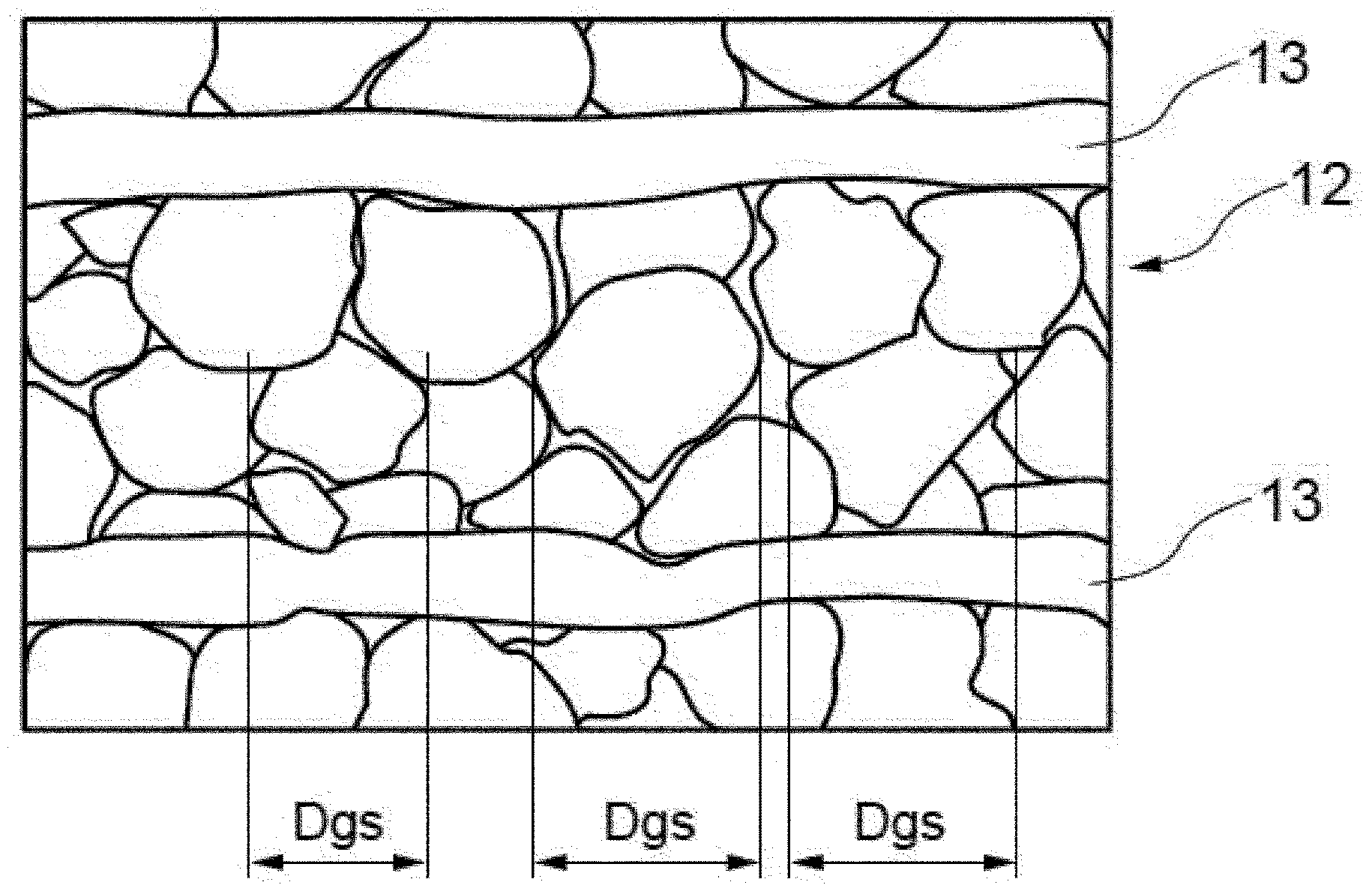
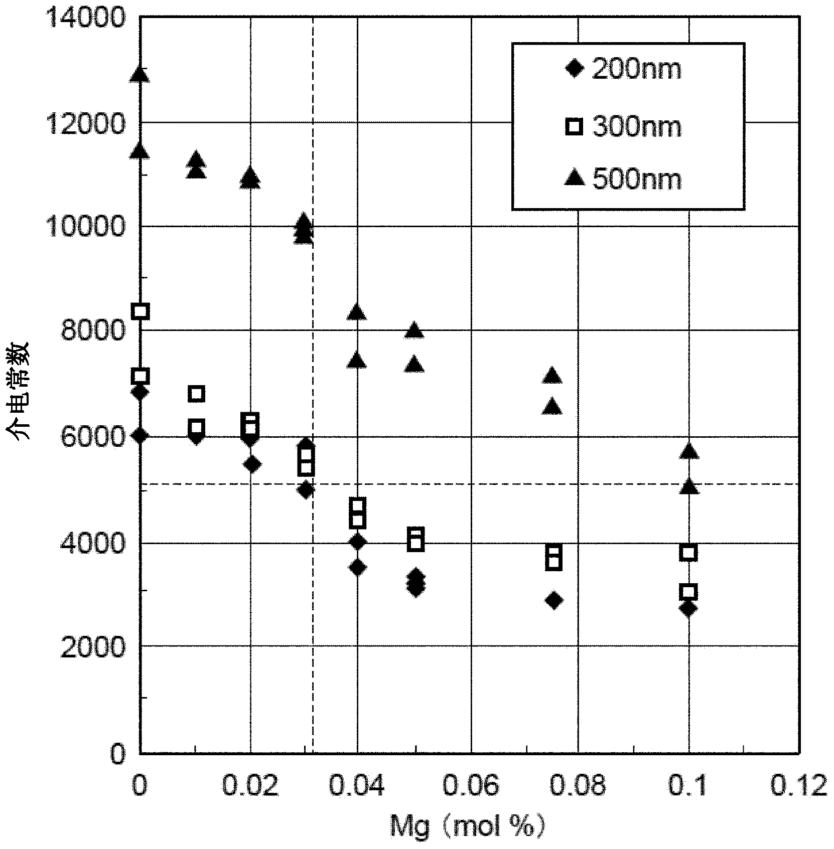
However, if the particle size of the dielectric is reduced while the dielectric layer is thinned, the dielectric constant will decrease due to the size effect, and a sufficient capacity cannot be obtained as a capacitor as a whole.

Method used


Image

  • Laminated ceramic capacitor
  • Laminated ceramic capacitor
  • Laminated ceramic capacitor

Examples


Embodiment

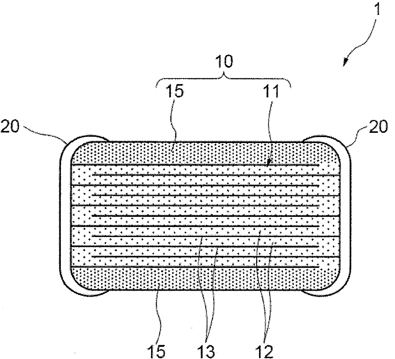
[0038] Next, examples of the multilayer ceramic capacitor (hereinafter referred to as "MLCC") of the present invention will be described.

[0039]

[0040] (1) Preparation of dielectric raw material powder

[0041] First, as the raw material powder of the dielectric, high-purity BaTiO with an average particle size of 110 nm 3 Powder, ReO shown in Tables 1 to 7 3 / 2 , SiO 2 , MO X (to be used as MnCO 3 ; by roasting CO 2 Separation into MnO), ZrO 2 Each compound of MgO and MgO is prepared as a raw material powder for a dielectric. The average particle diameter of the raw material powder was obtained by observing the powder samples of barium titanate with SEM, the number of samples was 500, and the median particle diameter was taken. Next, the respective compounds were weighed and mixed so that the composition ratio of the dielectric layer of the MLCC, that is, the sintered body became the composition ratio shown in Tables 1-7. The raw material powders of the respective...


PUM

PropertyMeasurementUnit
particle sizeaaaaaaaaaa
diameteraaaaaaaaaa
thicknessaaaaaaaaaa

Abstract

By suppressing grain growth, which occurs when dielectric particles constituting a dielectric layer are fired to maintain grain boundaries, and by setting permittivity per unit grain size to a high value, high density laminated layers and improved reliability are both achieved in this laminated ceramic capacitor. The laminated ceramic capacitor has a dielectric layer constituting a sintered body containing, with respect to 100 moles of BaTiO3, amols of ReO3 / 2, bmols of SiO2, cmols of MOx, dmols of ZrO2, and emols of MgO (where Re is a rare earth element, M is a metal element (excluding Ba, Ti, Re, Si, Zr, Mg and rare earth elements), and x is a valence). The aforementioned a, b, c, d and e, which represent the number of moles of each component, are 0.1 <= a <= 1.0, 0.1 <= b <= 1.5, 0.1 <= c <= 0.4, 0 <= d <= 1.0, and 0 <= e <= 0.03.

Description

technical field [0001] The present invention relates to a multilayer ceramic capacitor (MLCC) capable of achieving a smaller and larger capacity by stacking dielectric layers at a high density. Background technique [0002] With the miniaturization and thinning of digital electronic devices such as mobile phones, in the multi-layer ceramic capacitor (MLCC: Multi-Layer ceramic capacitor) mounted on the electronic circuit board, the miniaturization and increase in the required chip size and capacity The demand is increasing year by year. In general, when the size of a capacitor is reduced, the area of ​​the internal electrodes facing the dielectric layer inevitably becomes smaller, thereby reducing the capacitance. Therefore, in order to achieve miniaturization of the chip size and secure the capacity of the capacitor, a high-density lamination technology of making the dielectric layer between the internal electrodes thin and stacking the dielectric layers in multiple layers ...

Claims


Application Information

Patent Timeline
Patent Type & Authority Applications(China)
IPC IPC(8): H01G4/12C04B35/468H01G4/30
CPCC04B2235/3418C04B2235/3239C04B2235/5445C04B2235/3206C04B35/4682H01G4/1227C04B2235/663C04B2235/6025C04B35/64C04B2235/6584C04B2235/3262C04B2235/3224C04B2235/658C04B2235/3225C04B2235/3244C04B2235/781C04B2235/785H01G4/10H01G4/1236H01G4/20H01G4/224H01G4/30
Inventor 森田浩一郎志村哲生长冈邦彦
Owner TAIYO YUDEN KK
Learn More