Preparation method of SERS (Surface-Enhanced Raman Scattering) chip

A chip and pit technology, applied in the field of SERS chip preparation, can solve the problems of difficulty in meeting detection requirements, limited output and high production cost, and achieve the effects of good SERS activity, low cost and good uniformity

Active Publication Date: 2018-11-23
苏州英菲尼纳米科技有限公司
View PDF35 Cites 8 Cited by
  • Summary
  • Abstract
  • Description
  • Claims
  • Application Information

AI Technical Summary

Problems solved by technology

However, for SERS substrates with excellent SERS activity and uniformity, the production cost is often high, and the output is limited, which is difficult to meet the daily detection needs.

Method used


Image

  • Preparation method of SERS (Surface-Enhanced Raman Scattering) chip
  • Preparation method of SERS (Surface-Enhanced Raman Scattering) chip
  • Preparation method of SERS (Surface-Enhanced Raman Scattering) chip

Examples


Embodiment 1

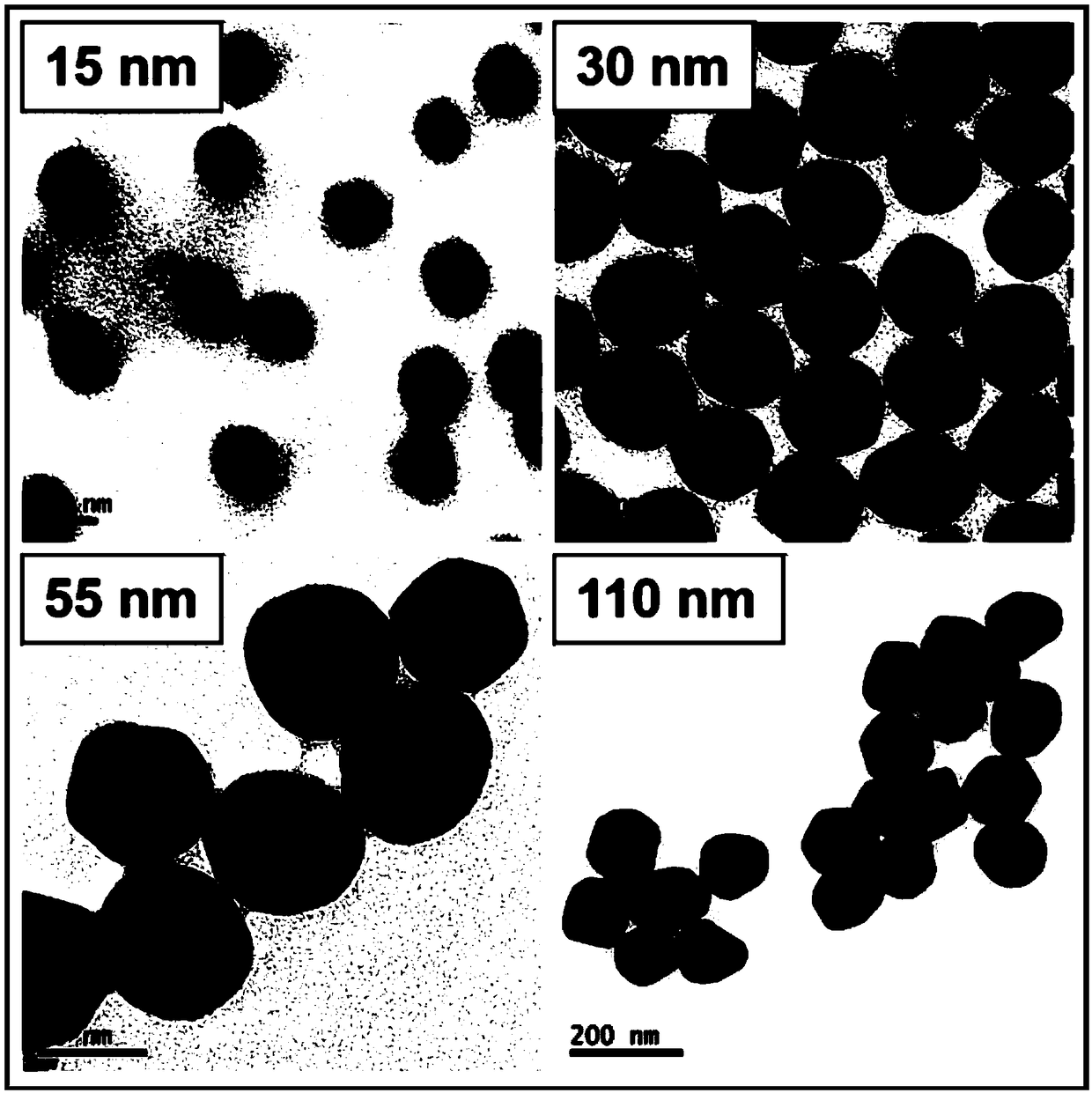
[0071] 1mL HAuCl 4 (25mM) was diluted to 100mL, heated to boiling, and 750uL of sodium citrate aqueous solution (1.14g diluted to 100mL) was added under vigorous stirring. Continue heating for 15 minutes to obtain Au sol with a particle size of 50 nm and a concentration of about 7.5×10 9 individual / mL. The size of the obtained Au nanoparticles can be adjusted by changing the amount of sodium citrate added. figure 1 The TEM images of several Au nanoparticles with different sizes are shown, among which, the upper left image is the TEM image of Au nanoparticles with a particle size of 15nm prepared by adding 2000uL sodium citrate, and the upper right image is the particle obtained by adding 1000uL sodium citrate. The TEM image of Au nanoparticles with a diameter of 30nm, the lower left image is the TEM image of Au nanoparticles with a particle size of 55nm prepared by adding 700uL sodium citrate, and the lower right image is the particle size of 110nm prepared with 300uL sodium...

Embodiment 2

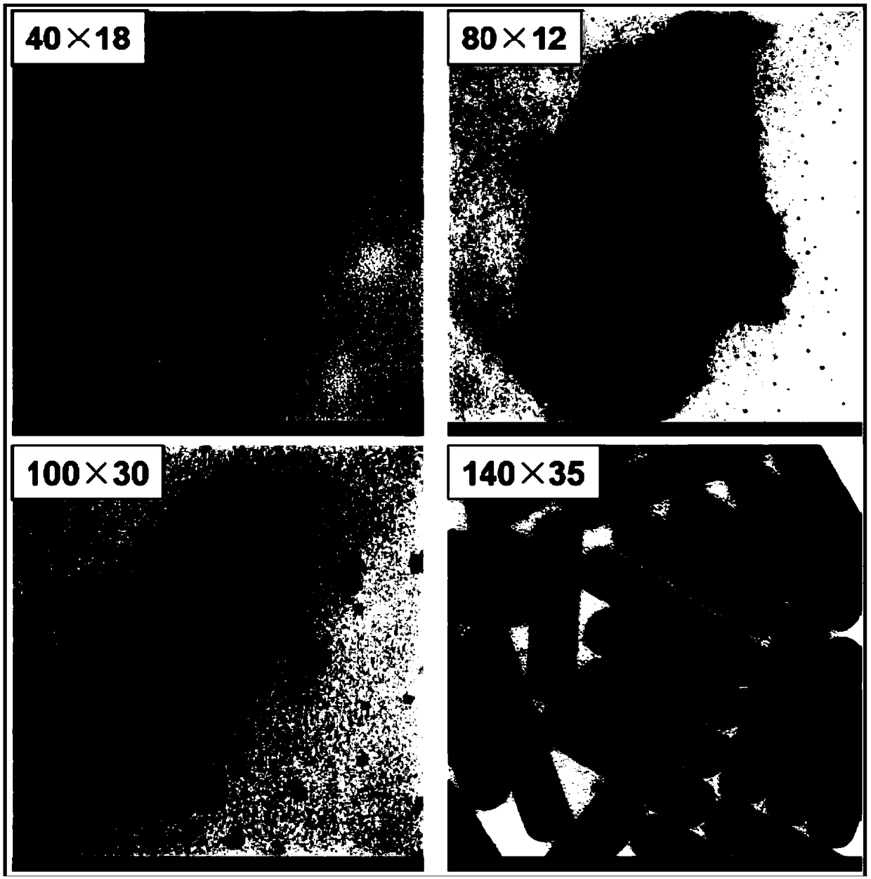
[0073] Seed preparation: Dissolve 0.3645g CTAB (cetyltrimethylammonium bromide) in 9.9mL water, dissolve in water bath at 60°C, add 100uL 1% (w / v%) HAuCl after cooling to 30°C 4 aqueous solution; add 1 mL of 6 mM NaBH with vigorous stirring 4 Aqueous solution, after stirring vigorously for 2 minutes, let stand for 30 minutes before use. Seed growth: 0.9g CTAB and 0.1400g sodium oleate were dissolved in 25mL water, dissolved in a water bath at 60°C, and cooled to 30°C. Add 1.8mL 4mM AgNO 3 Aqueous solution, let stand for 15min, add 25mL 1mM HAuCl at 700rpm 4 Aqueous solution, stir for 90min; add 150uL concentrated hydrochloric acid, and continue stirring at 400rmp for 15min. Finally, 125uL of 0.064MAA (ascorbic acid) aqueous solution was added, vigorously stirred for 30s, 40uL of seeds were added, vigorously stirred for 30s and then left to stand for 12h, finally rod-shaped Au nanoparticles were obtained. The size of the final nanorods can be controlled by adjusting the amo...

Embodiment 3

[0077] Step (1), providing a solid phase template with pits formed on the surface;

[0078] Step (2), the nanoparticle concentration that embodiment 1 makes is about 7.5 * 10 9 A / mL dilute solution was concentrated to obtain a nanoparticle concentration of about 1×10 11 A / mL ink;

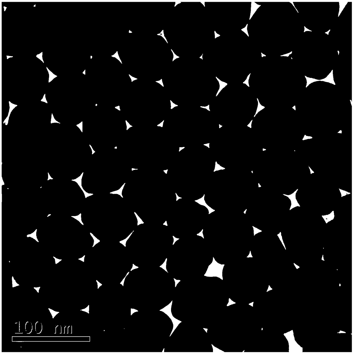
[0079] Step (3), spray the ink obtained in step (2) onto the solid-phase stencil of step (1) with ultrasonic spraying equipment, the number of sprays is 2 times, the ambient temperature during spraying is 25 ° C, and dry to obtain the SERS chip, For a TEM image of the chip see Figure 4 .


PUM

PropertyMeasurementUnit
diameteraaaaaaaaaa
diameteraaaaaaaaaa
particle sizeaaaaaaaaaa

Abstract

The invention provides a preparation method of an SERS (Surface-Enhanced Raman Scattering) chip. By an ultrasonic spray coating method, a dispersion solution containing metal nanometer particles is sprayed and coated onto the surface of a substrate with a plurality of concave pits on the surface; solvents of the dispersion solution are removed through volatilization, so that the metal nanometer particles are self-assembled in the concave pits of the substrate. The ultrasonic spray coating is used for preparing the SERS chip; the cost is low; the high-quality SERS chip can be prepared at high flux; the SERS chip prepared by the method has good SERS activity, ultrahigh uniformity, batch reproducibility and ultrahigh stability, and can be used for trace substance detection.

Description

technical field [0001] The invention relates to Surface-Enhanced Raman Scattering (SERS) technology, in particular to a method for preparing a SERS chip. Background technique [0002] Surface-Enhanced Raman (Surface-Enhanced Raman Scattering, SERS) is through the interaction between the probe molecules on or near the surface of the metal nanostructure and the metal surface to generate Raman-enhanced scattering (Surface Plasmon Resonance, SPR), and SERS produces The Raman signal will be enhanced by 10 compared with ordinary Raman scattering 3 -10 14 times. Compared with other spectral detection methods, SERS has three obvious advantages of high sensitivity, high selectivity and loose detection conditions, and can be widely used in many fields such as trace analysis, single molecule detection, biomedical detection, surface adsorption and catalytic reaction. [0003] The level of SERS activity depends on the nanostructure of the substrate, which is closely related to its sha...

Claims


Application Information

Patent Timeline
Patent Type & Authority Applications(China)
IPC IPC(8): G01N21/65B82Y30/00
CPCB82Y30/00G01N21/658
Inventor 郭清华孙海龙
Owner 苏州英菲尼纳米科技有限公司
Why Eureka
Try Eureka