High-power LED packaging structure

A LED packaging and high-power technology, which is applied in the direction of electrical components, circuits, semiconductor devices, etc., can solve problems such as difficulty in controlling the shape and uniformity of phosphor powder, intensifying the reabsorption of LED chips, and reducing external quantum efficiency, so as to facilitate industrialization The effect of production, improvement of light distribution performance, and simple structure

Inactive Publication Date: 2012-09-26
SHAANXI UNIV OF SCI & TECH
View PDF4 Cites 3 Cited by
  • Summary
  • Abstract
  • Description
  • Claims
  • Application Information

AI Technical Summary

Problems solved by technology

This structure is difficult to control the shape and uniformity of the phosphor, and it is easy to cause problems such as uneven distribution of light intensity and uneven color distribution.
And the phosphor layer is too close to the LED chip, which intensifies the reabsorption of the LED chip and reduces the external quantum efficiency.

Method used


Image

  • High-power LED packaging structure
  • High-power LED packaging structure
  • High-power LED packaging structure

Examples


Embodiment

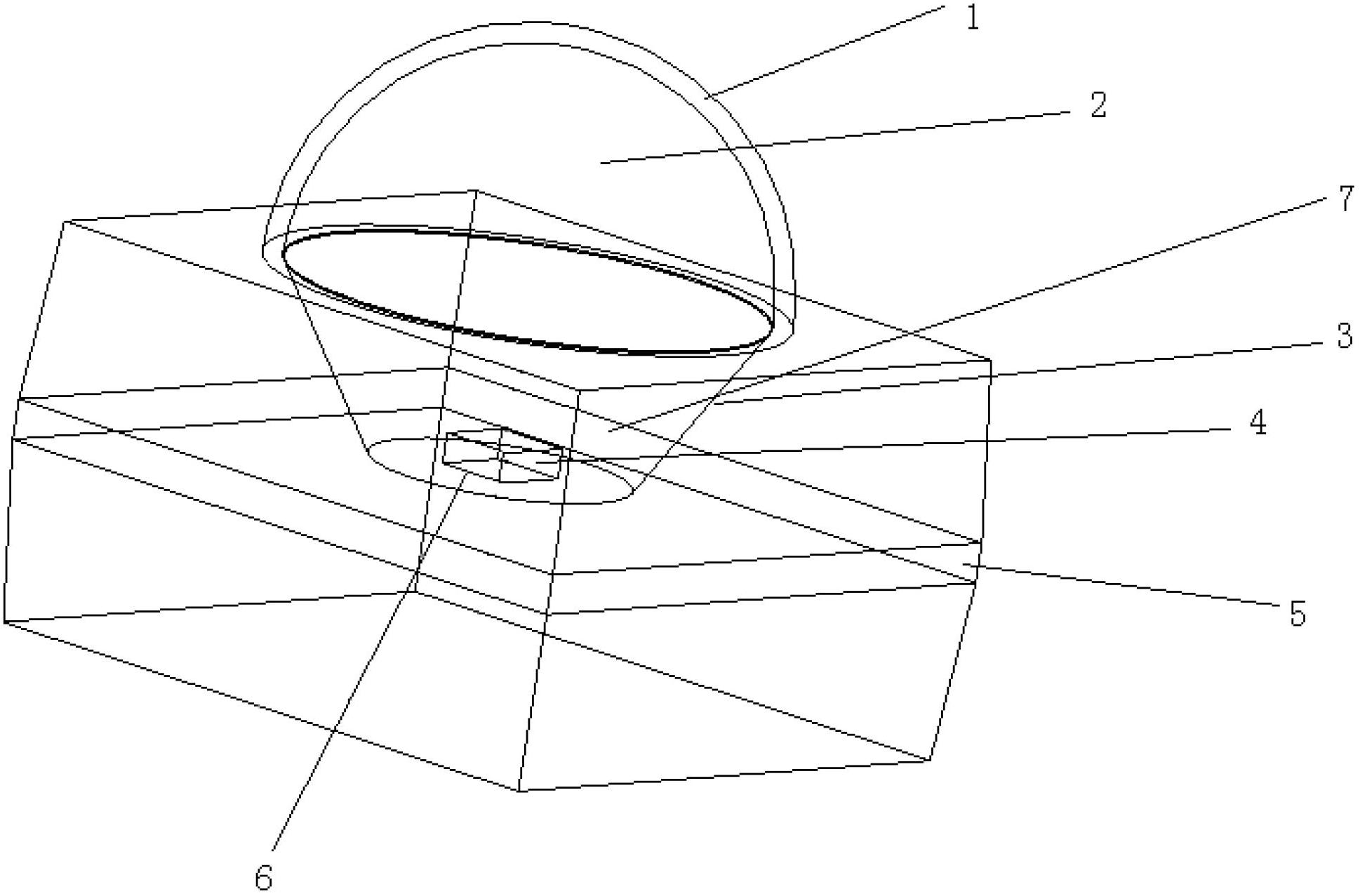
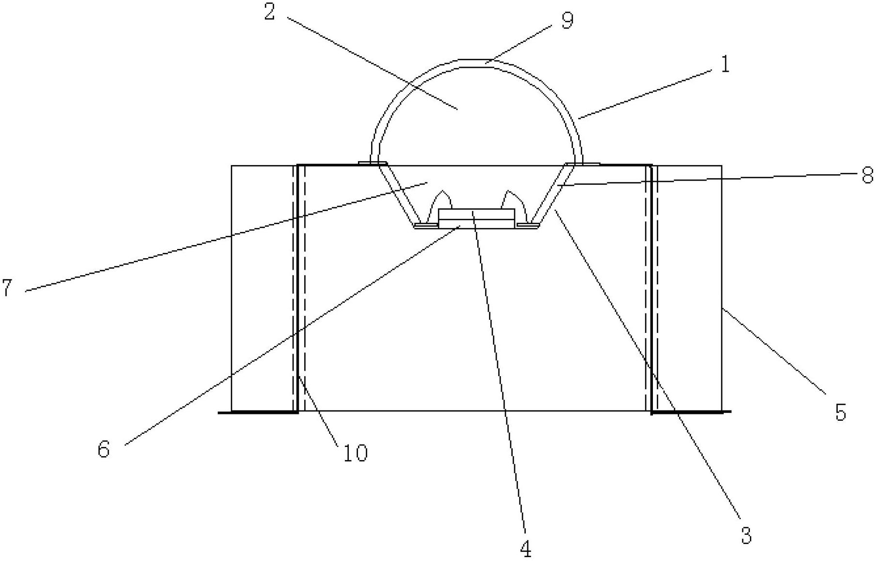
[0024] A high-power LED packaging structure adopts an integrated packaging structure, the power of the LED chip used is 1-3W, the thickness of the phosphor layer is 1-3mm, and the height of the dispensing layer is 2-4mm. During preparation, the reflective cup is first manufactured on the metal aluminum plate, and then the surface of the metal aluminum plate is insulated, and then electrodes are fixed on the reflective cup to complete the integrated packaging substrate. Then carry out the traditional packaging steps for the LED chip, crystal expansion-spine-short baking, so that the LED chip is solidified in the reflective cup on the integrated packaging substrate through the bonding layer; the connection between the electrode and the chip is completed by punching gold wires; manufacturing After the hemispherical phosphor layer, dispensing, dispensing, and long baking are carried out on the LED chip, and finally the lens and the metal aluminum plate are fixed by filling the enca...


PUM


Abstract

The invention provides a high-power LED packaging structure. The high-power LED packaging structure comprises a reflective cup and an integrated packaging substrate, wherein the reflective cup is a groove formed on the surface of the integrated packaging substrate; a lens is arranged at the upper end of the reflective cup; a bonding layer, an LED chip, a dispensing layer and a phosphor powder layer are sequentially arranged in a cavity formed by the lens and the reflective cup; and an electrode for connecting the LED chip and a drive circuit is arranged on the integrated packaging substrate. The LED packaging structure provided by the invention adopts integrated package to avoid heat dissipation bottleneck in traditional LEDs; and the layered dispensing layer enables the LED chip to be far away from the phosphor powder layer, so that light re-absorption of the LED chip in the traditional packaging structure is reduced, and the light emitting rate and the light distribution performance are improved. The LED packaging structure provided by the invention not only has a simple structure but also omits a bracket, an aluminum baseplate and a heat sink part in traditional package, thereby reducing the process steps, lowering the cost and facilitating industrial production.

Description

technical field [0001] The invention relates to an LED packaging structure, in particular to a high-power LED packaging structure. Background technique [0002] LED is a kind of diode that uses semiconductor PN junction to emit light. It has a broad market in the fields of indicator lights, signal lights, backlights, and landscape lighting. LED has the advantages of high luminous efficiency, low power consumption, long service life, strong safety and reliability, and environmental protection, making it the fourth-generation lighting source to replace traditional incandescent lamps, fluorescent lamps, and high-pressure gas discharge lamps. The packaging structure of the LED will directly affect the core issues such as the junction temperature and light distribution performance of the LED, so the scientific light distribution performance is a breakthrough to improve the heat dissipation and light distribution of the LED. [0003] The packaging of traditional high-power LEDs ...

Claims


Application Information

Patent Timeline
Patent Type & Authority Applications(China)
IPC IPC(8): H01L33/48H01L33/50H01L33/64H01L33/54
Inventor 张方辉邱西振
Owner SHAANXI UNIV OF SCI & TECH
Why Eureka
Try Eureka