High-power LED packaging structure
An LED packaging, high-power technology, applied in electrical components, circuits, semiconductor devices, etc., can solve problems such as difficulty in controlling the shape and uniformity of phosphors, aggravating the reabsorption of LED chips, and reducing external quantum efficiency. Production, improve light distribution performance, the effect of simple structure
- Summary
- Abstract
- Description
- Claims
- Application Information
AI Technical Summary
Problems solved by technology
Method used
Image
Examples
Embodiment
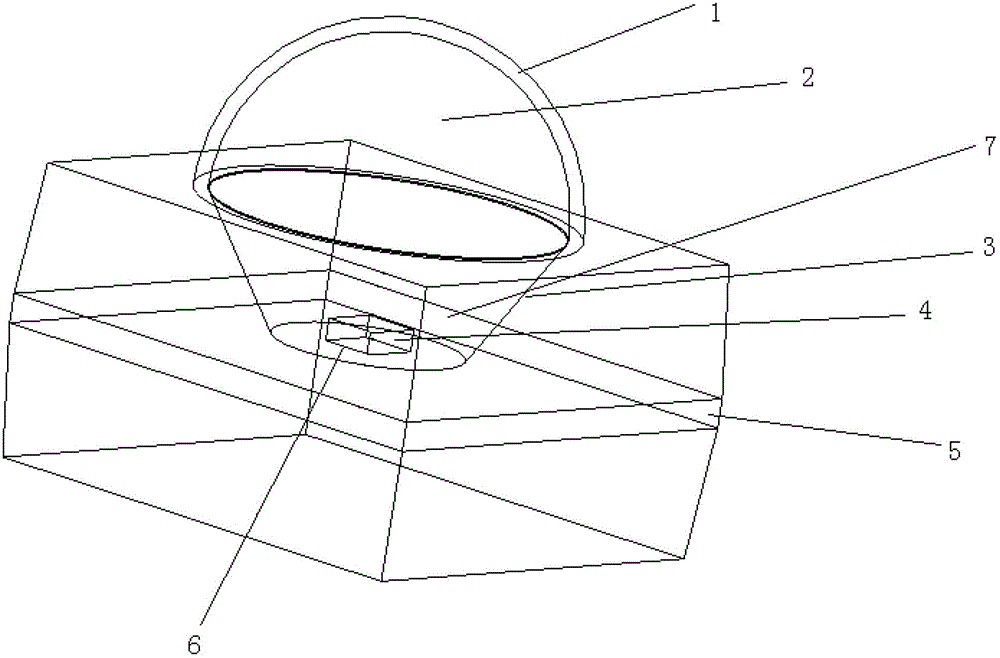
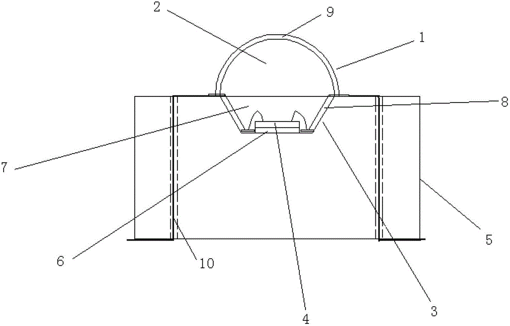
[0024] A high-power LED packaging structure adopts an integrated packaging structure, the power of the LED chip used is 1-3W, the thickness of the phosphor layer is 1-3mm, and the height of the dispensing layer is 2-4mm. During preparation, the reflective cup is first manufactured on the metal aluminum plate, and then the surface of the metal aluminum plate is insulated, and then electrodes are fixed on the reflective cup to complete the integrated packaging substrate. Then carry out the traditional packaging steps for the LED chip, crystal expansion-spine-short baking, so that the LED chip is solidified in the reflective cup on the integrated packaging substrate through the bonding layer; the connection between the electrode and the chip is completed by punching gold wires; manufacturing After the hemispherical phosphor layer, dispensing, dispensing, and long baking are carried out on the LED chip, and finally the lens and the metal aluminum plate are fixed by filling the enca...
PUM
 Abstract
Description
Claims
Application Information


