Eureka AIR delivers breakthrough ideas for toughest innovation challenges, trusted by R&D personnel around the world.

Opto-electric hybrid board and manufacturing method therefor

A technology of optoelectronic hybrid substrate and manufacturing method, applied in final product manufacturing, sustainable manufacturing/processing, optics, etc., can solve problems such as increased cost, time-consuming and labor-intensive, and poor alignment accuracy.

Inactive Publication Date: 2012-10-03
NITTO DENKO CORP
View PDF6 Cites 2 Cited by
  • Summary
  • Abstract
  • Description
  • Claims
  • Application Information

AI Technical Summary

Problems solved by technology

[0007] However, in the alignment method of the above-mentioned Patent Document 1, although high-precision alignment can be performed, it is time-consuming and labor-intensive, and lacks in mass production.
In addition, in the centering method of the above-mentioned Patent Document 2, although the alignment can be performed by a simple method such as fitting the hole and the pin, not only dimensional error occurs when the connector and the pin are separately manufactured, but also the connector Due to the positional deviation with respect to the mounting position of the optical waveguide unit, and the positional deviation of the positioning pins with respect to the mounting position of the circuit unit, these dimensional errors and positional deviations accumulate, and the alignment accuracy deteriorates.
Therefore, when it is desired to improve the alignment accuracy, it is necessary to manage the dimensional accuracy so that the above-mentioned dimensional error and positional deviation do not occur, so the cost is increased, and the mass production is lacking.

Method used


Image

  • Opto-electric hybrid board and manufacturing method therefor
  • Opto-electric hybrid board and manufacturing method therefor
  • Opto-electric hybrid board and manufacturing method therefor

Examples


Embodiment 1

[0076] Fabrication of Optical Waveguide Units

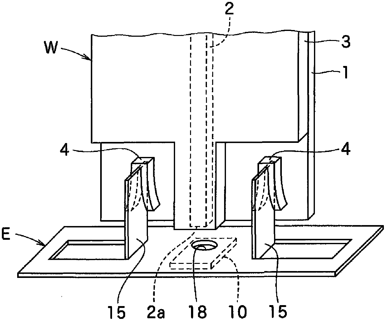
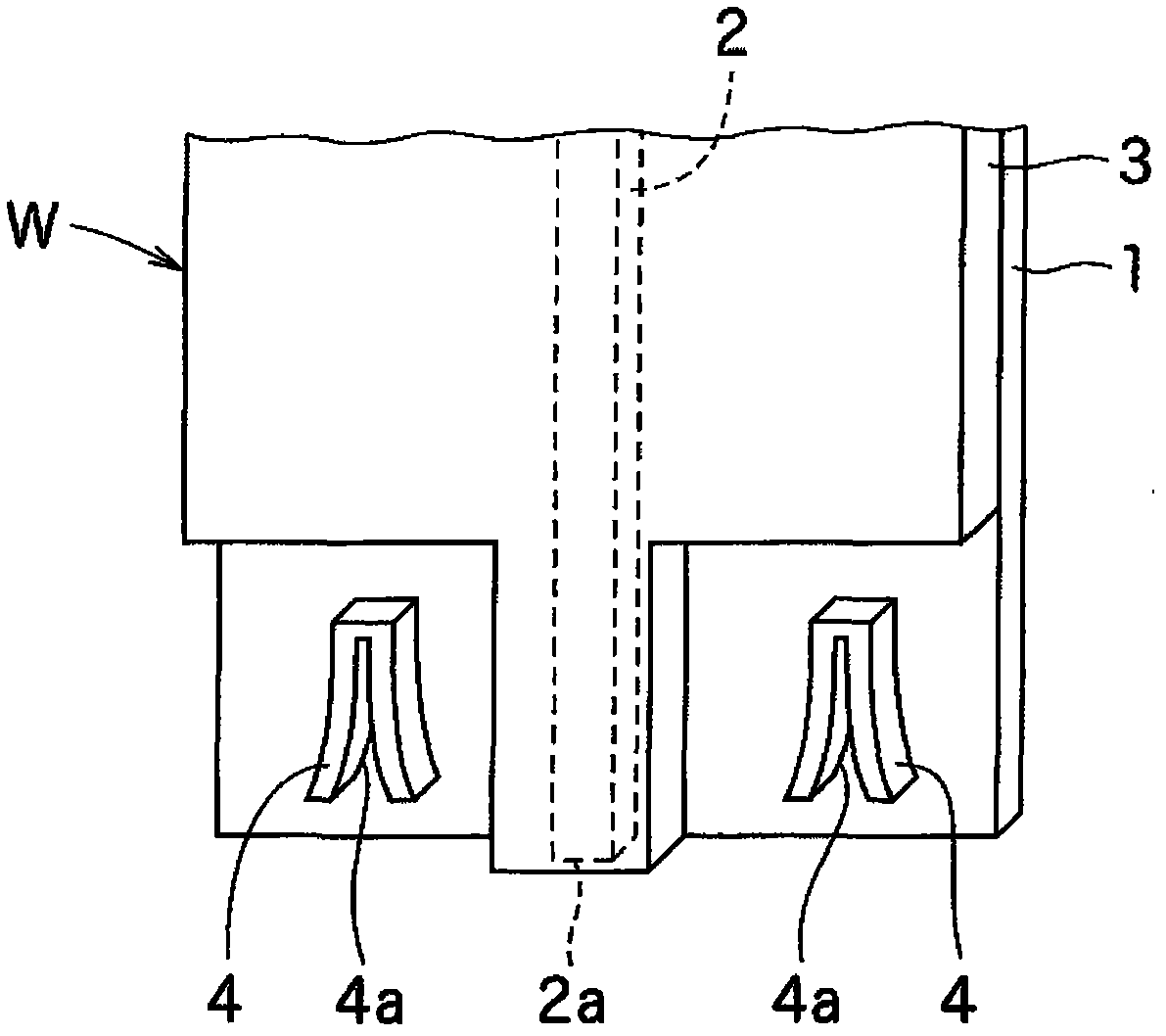
[0077] Using each of the above-mentioned materials for forming the lower cladding layer, core, and upper cladding layer, in order to be compatible with the above-mentioned figure 1 An optical waveguide unit having a V-shaped insertion portion for positioning a circuit unit was manufactured in the same manner as the illustrated embodiment. The dimension of the above-mentioned V-shaped insertion part is 1.98 mm in depth, the minimum width of the inner side of the V-shape is 80 μm, the maximum width of the opening side of the V-shaped opening is 820 μm, and the center of the adjacent insertion part The distance between them is 6.0mm.

[0078] Fabrication of circuit units

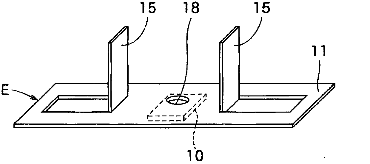
[0079] with the above figure 1 A circuit unit having a rectangular bent portion that fits into the insertion portion for positioning the circuit unit described above was fabricated by the same method as in the illustrated embodiment. The dimensions of the ...

Embodiment 2

[0083] Fabrication of Optical Waveguide Units

[0084] One end of the optical waveguide unit of Embodiment 1 described above and Figure 9 of (a), Figure 9 The embodiment shown in (b) is similarly formed as an inclined surface. The other parts are the same as in the above-mentioned Example 1.

[0085] Fabrication of circuit units

[0086] The circuit unit of Embodiment 1 described above was prepared.

[0087] Manufacture of photoelectric hybrid substrate

[0088] The optical waveguide unit and the circuit unit are integrated by fitting the bent portion of the circuit unit into the insertion portion of the optical waveguide unit with the optical waveguide unit parallel to the circuit unit. Then, the fitting portion is fixed with an adhesive.

[0089] light propagation test

[0090] Electricity was supplied to the light-emitting elements of the photoelectric hybrid substrates of Examples 1 and 2 above to emit light from the light-emitting elements. Then, it was ...

Embodiment 3

[0092] Fabrication of Optical Waveguide Units

[0093] In addition to the optical waveguide unit of the above-mentioned first embodiment, the other end portion is also an optical waveguide unit having a V-shaped insertion portion for positioning the circuit unit in the same manner as the one end portion. The other parts are the same as in the above-mentioned Example 1.

[0094] Fabrication of circuit units

[0095] The same circuit unit as in Embodiment 1 above was produced. Furthermore, a circuit unit in which a flip-chip type light-receiving element (manufactured by Albis Corporation, PDCA04-70-GS) was mounted instead of the light-emitting element in the circuit unit of Example 1 was produced.

[0096] Manufacture of photoelectric hybrid substrate

[0097] In the same manner as in the first embodiment, the circuit unit of the light-emitting element was fixed to one end of the optical waveguide unit, and the circuit unit of the light-receiving element was fixed to th...


PUM


Abstract

Provided are an opto-electric hybrid board and a manufacturing method. The opto-electric hybrid board includes an optical waveguide unit and an electric circuit unit (W) having an optical element (10) mounted thereon. The optical waveguide unit (W) includes socket portions for locating the electric circuit unit, which are formed on a surface of an undercladding layer and formed of the same material as a core. The socket portions are located at predetermined locations with respect to one end surface of a core. The electric circuit unit (E) includes bent portions (15)which are formed by bending a part of an electric circuit board so as to stand, for fitting into the socket portions. The bent portions (15) are located at predetermined locations with respect to the optical element. The optical waveguide unit (W) and the electric circuit unit (E)are coupled in a state in which the bent portions (15) fit into the socket portions( 4).

Description

technical field [0001] The present invention relates to a photoelectric hybrid substrate having an optical waveguide unit and a circuit unit on which optical elements are mounted and a manufacturing method thereof. Background technique [0002] In recent electronic equipment and the like, as the amount of information to be transmitted increases, optical wiring is used in addition to electrical wiring. That is, an opto-electric hybrid board having a circuit unit and an optical waveguide unit in which a light-emitting element for converting an electrical signal into an optical signal is mounted on a circuit board on which electrical wiring is formed is incorporated in the above-mentioned electronic equipment, etc. and an optical element such as a light receiving element for converting an optical signal into an electrical signal; the optical waveguide unit is formed with an optical waveguide as an optical wiring for transmitting the above-mentioned optical signal. [0003] In ...

Claims


Application Information

Patent Timeline
Patent Type & Authority Applications(China)
IPC IPC(8): G02B6/42G02B6/122G02B6/13
CPCG02B6/138H05K2201/09072G02B6/42H05K1/181H05K2201/09063G02B6/4214H05K1/0274H05K2201/09081H05K3/002G02B6/4257G02B6/423G02B6/428H05K2201/10121Y10T29/49126Y10T29/49Y02P70/50
Inventor 长藤昭子辻田雄一程野将行井上真弥
Owner NITTO DENKO CORP
Why Eureka
Eureka Blog
Learn More