Liquid crystal grating, manufacturing method of liquid crystal grating, 3D display part and 3D display device

A technology of liquid crystal grating and manufacturing method, which is applied to optical components, static indicators, optics, etc., and can solve problems such as scratches on the Sensor surface, reduced production capacity, and interference

Active Publication Date: 2012-10-03
BEIJING BOE OPTOELECTRONCIS TECH CO LTD
View PDF3 Cites 13 Cited by
  • Summary
  • Abstract
  • Description
  • Claims
  • Application Information

AI Technical Summary

Problems solved by technology

[0005] 1. If the 3D part 2 and the touch part 3 are simply and mechanically integrated, that is, using the Add On external touch screen + 3D display module, it will lead to problems such as complicated production process and high production cost, and the whole module The thickness of the group is relatively large, which will inevitably affect the 3D display effect
[0006] 2. Use figure 1 In the structure shown, there is a large signal interference between the touch part 3 and the 3D part 2
When the strip electrode 25 is grounded and the surface electrode 26 transmits alternating current, because the current of the surface electrode 26 is transmitted through the conductive rubber TR outside the plastic frame 21 on the peripheral circuit of the upper substrate 22, and the peripheral wiring and the touch electrode layer 31 are in the vertical direction There is an overlapping portion on the top, causing the alternating current in the surface electrode 26 to cause signal interference to the touch component 3
Conversely, when the strip electrode 25 transmits alternating current and the surface electrode 26 is grounded, since the strip electrode 25 and the touch electrode layer 31 have overlapping portions in the vertical direction, the alternating current in the strip electrode 25 will generate a severe signal interference
[0007] 3. In the prior art, the FPC (Flexible Printed Circuit board, flexible printed circuit board) welding area (Bonding) position of the touch component 3 is suspended ( figure 1 As shown by the dotted circle in the middle), it is not easy to correspond to BondingFPC
[0012] From the perspective of the process flow, when making the 3D grating + On Cell Touch structure in the prior art, if the Sensor layer is first made on the upper surface of the upper substrate, and then the 3D layer is made, in this case, when forming the metal layer of the 3D layer, It is possible to etch off the gold finger of FPC Bonding in the touch control part
Moreover, during this process, the Sensor surface contacts the transport rollers too much, and if no protective measures are taken, it is easy to cause the Sensor surface to be scratched
If the 3D layer is made first and then the Sensor layer is made, the upper substrate (such as a glass substrate) will be flipped twice (once for the process and once for the alignment). Since the existing technology requires manual flipping of the upper substrate, this will not only increase the number of flips, reduce The production capacity is reduced, and manual flipping will cause scratches
If the 3D metal layer is made on the upper substrate first, then the Sensor layer is made, and then the 3D ITO layer is made, although this can reduce the number of substrate flips during alignment, but the substrate also needs to be flipped twice during the process.
[0013] To sum up, the 3D grating + On Cell Touch structure in the prior art has a large signal interference problem, and the number of times the substrate is turned over during the production process will inevitably cause more scratches on the substrate

Method used


Image

  • Liquid crystal grating, manufacturing method of liquid crystal grating, 3D display part and 3D display device
  • Liquid crystal grating, manufacturing method of liquid crystal grating, 3D display part and 3D display device
  • Liquid crystal grating, manufacturing method of liquid crystal grating, 3D display part and 3D display device

Examples


Embodiment Construction

[0035] The main realization principles, specific implementation methods and corresponding beneficial effects that can be achieved of the technical solutions of the embodiments of the present invention will be described in detail below in conjunction with each accompanying drawing.

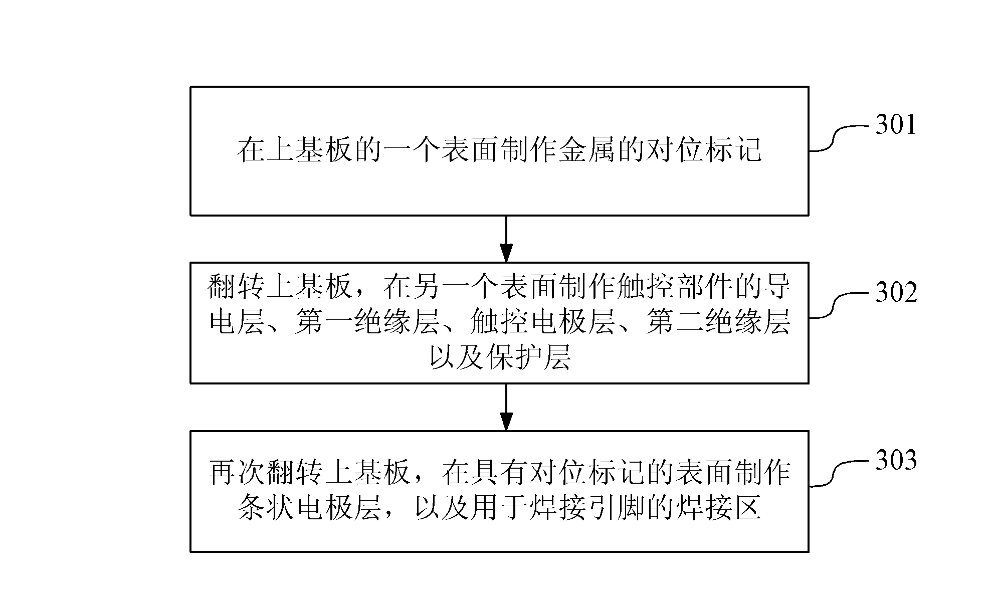
[0036] In order to solve the problems existing in the prior art, an embodiment of the present invention provides a method for fabricating a liquid crystal grating, such as Figure 4 As shown, the method includes:

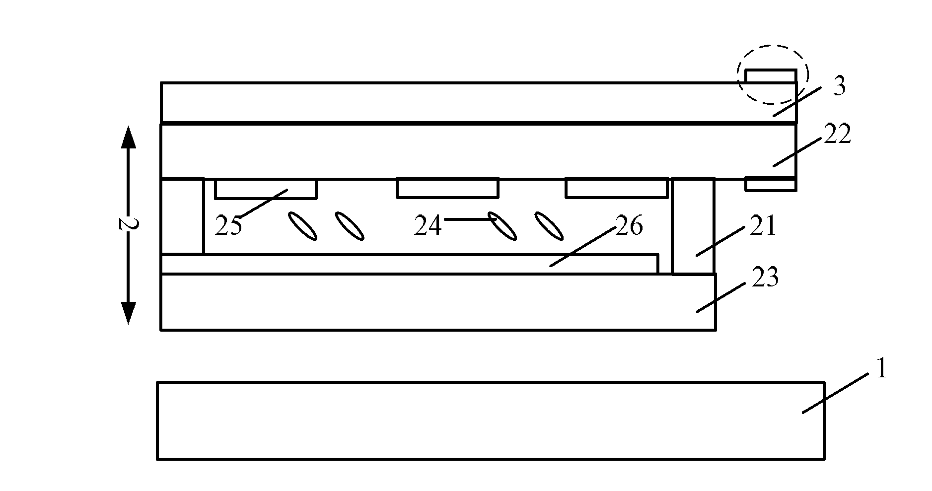
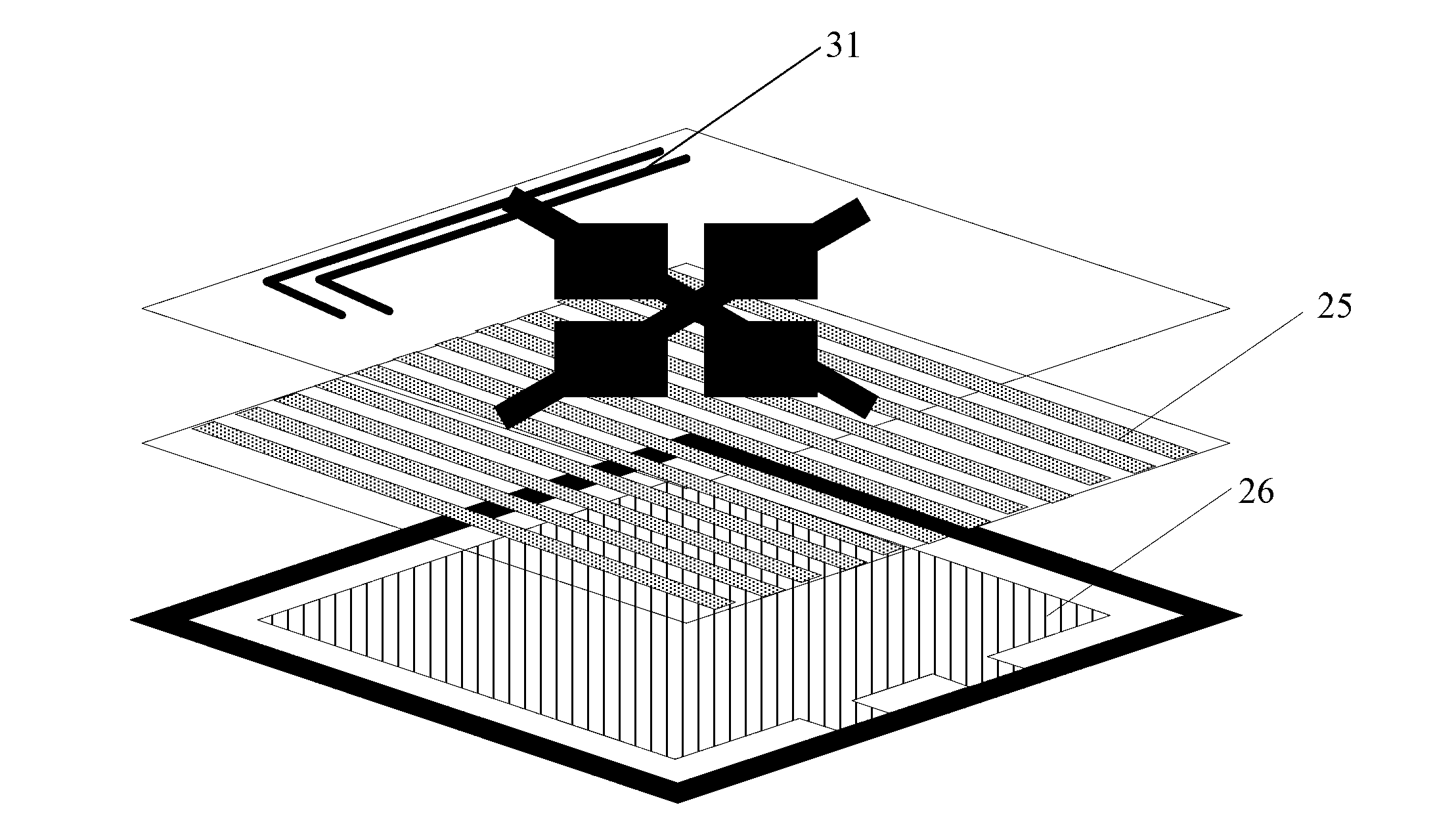
[0037] Step 401, making a conductive layer and an alignment mark on the upper surface of the upper substrate according to the first preset image;

[0038] Step 402, sequentially fabricating a first insulating layer, a touch electrode layer and a second insulating layer on the conductive layer;

[0039] Step 403, making a surface electrode on the lower surface of the upper substrate, and the surface electrode is grounded;

[0040] Step 404 , aligning the upper substrate and the lower su...


PUM


Abstract

The invention discloses a liquid crystal grating, a manufacturing method of the liquid crystal grating, a 3D (three-dimensional) display part and a 3D display device. The manufacturing method of the liquid crystal grating comprises the following steps: manufacturing a conducting layer and aligning marks on the upper surface of an upper base plate according to a first preset pattern, orderly manufacturing a first insulating layer, a touch-controlled electrode layer and a second insulating layer on the conducting layer, manufacturing a grounded facial electrode on the lower surface of the upper base plate, and enclosing the upper base plate and a lower base plate according to the aligning marks to form the liquid crystal grating, wherein the upper surface of the lower base plate is provided with strip-shaped electrodes. Due to the grounded facial electrode formed on the lower surface of the upper base plate in the liquid crystal grating, the signal interferences between the 3D control part and the touch-controlled part in the liquid crystal grating can be shielded. Moreover, the aligning marks are manufactured at the same time of manufacturing the conducting layer of the touch-controlled part, so that the time of rotating the upper base plate is reduced, and further, the possibility of scratching and abrading the surface of the upper base plate is lowered.

Description

technical field [0001] The invention relates to the field of display technology, in particular to a liquid crystal grating, a manufacturing method thereof, a 3D display device and a 3D display device. Background technique [0002] At present, 3D products and touch (Touch) technology products are increasingly sought after by consumers. With such a large demand, the integrated products of the two are also concerned by many module manufacturers. However, most of the prior art simply combine the two, and there are many problems in such a general combination. [0003] From a structural point of view, as figure 1 As shown, it is a schematic diagram of the structure of the existing 3D grating + on-cell touch screen (On Cell Touch). Wherein, it includes a display component 1 , a 3D component 2 and a touch sensor (Touch sensor) 3 attached to the display component 1 . The 3D component 2 includes an upper substrate 22 and a lower substrate 23 connected by a plastic frame 21, a liqui...

Claims


Application Information

Patent Timeline
Patent Type & Authority Applications(China)
IPC IPC(8): G02F1/133G02F1/1333G02F1/1343G02B27/22G06F3/041
CPCG02B27/22G02F1/292G02F1/133G02F1/13338G02F1/13471G06F2203/04103Y10T29/49155G06F3/0412G06F3/041G02F1/1335
Inventor 杨盛际吴俊纬王海生
Owner BEIJING BOE OPTOELECTRONCIS TECH CO LTD
Why Eureka
Try Eureka