Flexible organic light emitting transistor display device

A technology of light-emitting transistors and transistors, which is applied in the manufacture of electric solid-state devices, semiconductor devices, semiconductor/solid-state devices, etc., can solve the problems of high device drive voltage, low device efficiency, and poor charge injection effect, and achieve lower operating voltage, The effect of improving work efficiency and improving working life

Active Publication Date: 2012-10-03
常州第六元素半导体有限公司
View PDF5 Cites 34 Cited by
  • Summary
  • Abstract
  • Description
  • Claims
  • Application Information

AI Technical Summary

Problems solved by technology

Traditional ITO and other materials are not suitable for flexible devices based on plastic substrates due to their inherent brittleness and the need for high-temperature annealing.
And the traditional OLET structure is that the source and drain electrodes are directly in contact with the organic semiconductor layer, so it is difficult for carriers to inject into the semiconductor layer from the source and drain electrodes, that is, the potential barrier is relatively large, so the device driving voltage is large, and the device efficiency is not high, resulting in its charge poor injection

Method used


Image

  • Flexible organic light emitting transistor display device
  • Flexible organic light emitting transistor display device
  • Flexible organic light emitting transistor display device

Examples


Embodiment 1

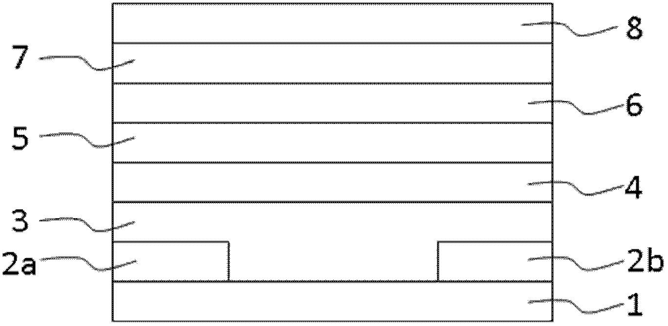
[0077] A flexible organic light-emitting transistor device structure includes: a substrate 1; source and drain electrode layers 2a and 2b; a charge injection layer 3; organic semiconductor layers 4, 5 and 6; a gate insulating layer 7; By using the novel charge injection layer 3, the charge injection capability can be improved, thereby improving the luminous efficiency of the device. Graphene is used as the source and drain electrodes, and as a bottom-emitting device, it has a very high aperture ratio. figure 1 It is a schematic cross-sectional structure diagram of the flexible organic light-emitting transistor device.

[0078] The fabrication process of the device mainly includes the following steps:

[0079] (1) The substrate 1 is cleaned.

[0080] (2) Use printing, spin coating, printing, transfer printing and other methods to prepare graphene on the surface of the flexible substrate as the source and drain electrode layer; at least ensure that some areas on the upper sur...

Embodiment 2

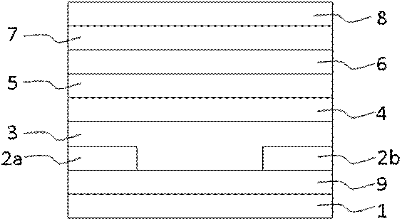
[0088] On the basis of the structure of the OLET provided in Example 1, an internal light extraction layer 9 is added. The extraction layer can be made of materials such as tantalum oxide, molybdenum oxide, tungsten oxide, vanadium oxide, etc., deposited on the substrate by sputtering, vacuum evaporation, etc. above the bottom. This layer structure can effectively extract the light emitted from the organic light-emitting layer to the inner surface of the substrate, so that more light can pass through the inner surface of the substrate and emit to the outer surface, thereby improving the working efficiency of the device, which is conducive to reducing the operating voltage of the device and improving the working efficiency of the device. Life-span, other each layer manufacturing method is identical with embodiment 1. figure 2 It is a schematic cross-sectional structure diagram of the flexible organic light-emitting transistor device described in Example 2.

[0089] It should ...

Embodiment 3

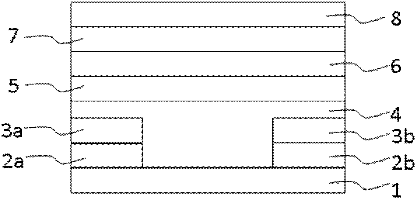
[0091] On the basis of the structure of the OLET provided in Example 1, corresponding independent electron and hole injection materials (injection layers) are respectively used. The charge injection layer uses two different types of charge injection materials 3a and 3b, which can achieve excellent electron injection and Hole injection, which greatly improves the working efficiency of the device, the hole injection layer can be molybdenum oxide, tungsten oxide, vanadium oxide, aluminum oxide, etc., and the material of the electron injection layer can be lithium fluoride, lithium oxide, zirconia, Titanium oxide, cesium carbonate etc., the preparation method of each layer is identical with embodiment 1. image 3 It is a schematic cross-sectional structure diagram of the flexible organic light-emitting transistor device described in Example 3.


PUM


Abstract

The invention relates to a flexible organic light emitting transistor display device, which comprises a substrate (1), a source electrode layer (2a), a drain electrode layer (2b), a charge injection layer (3), organic semiconductor layers (4, 5 and 6), a gate insulating layer (7) and a gate electrode layer (8), wherein the source and drain electrode layers (2a and 2b) are made of graphene. The charge injection layer is added, a charge injection material is selected, the drain and source electrode layers are made of the graphene, so that the flexible active matrix organic light emitting transistor display device is transparent and high in aperture opening ratio and brightness, low in operating voltage and long in service life.

Description

technical field [0001] The patent of the present invention relates to an organic light emitting display device, in particular to a flexible organic light emitting transistor display device. Background technique [0002] Since Dr. Deng Qingyun published an epoch-making paper on Organic light-emitting diode (OLED) devices in 1987 (Organic electroluminescent diodes, Tang, C.W.; Van Slyke, S.A., Applied Physics Letters (1987), 51 (12), 913-15.) After that, the research on organic light-emitting diode devices began to develop rapidly. Organic light-emitting diode display devices are all-solid-state devices with the advantages of thin thickness, high brightness, saturated colors, wide viewing angles, high contrast, and low power consumption. They can be used for color flat panel displays. Moreover, OLED is easy to realize flexible display, which makes it have unique advantages in competition with other display technologies, and is known as the next-generation display. [0003] W...

Claims


Application Information

Patent Timeline
Patent Type & Authority Applications(China)
IPC IPC(8): H01L27/32H01L51/50H01L21/77
CPCH10K50/30
Inventor 谭化兵王振中
Owner 常州第六元素半导体有限公司
Why Eureka
Try Eureka