Oxide semiconductor thin film transistor
An oxide semiconductor and thin film transistor technology, applied in transistors, semiconductor devices, electrical components, etc., can solve the problems of increasing the threshold voltage, high carrier concentration, affecting the working stability of oxide semiconductor thin film transistors, etc. achieve high stability
- Summary
- Abstract
- Description
- Claims
- Application Information
AI Technical Summary
Problems solved by technology
Method used
Image
Examples
Embodiment 1
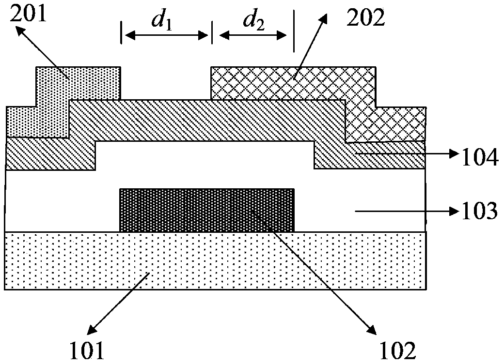
[0035] Such as figure 2 As shown, this embodiment provides an oxide semiconductor thin film transistor, including a substrate 101, a gate electrode 102, an insulating dielectric layer 103, and an oxide semiconductor channel layer 104 sequentially arranged on the substrate 101. The insulating dielectric layer 103 insulates the gate electrode 102 from the oxide semiconductor channel layer 104, the upper surface of the oxide semiconductor channel layer 104 is provided with a drain electrode 201 and a source electrode 202, and the drain electrode 201 and the source electrode The gap between 202 is d 1 , the length of the overlapping region between the source electrode 202 and the gate 102 in the horizontal direction is d 2 The contact between the source electrode 202 and the oxide semiconductor channel layer 104 is a Schottky contact, and the contact between the drain electrode 201 and the oxide semiconductor channel layer 104 is an ohmic contact.
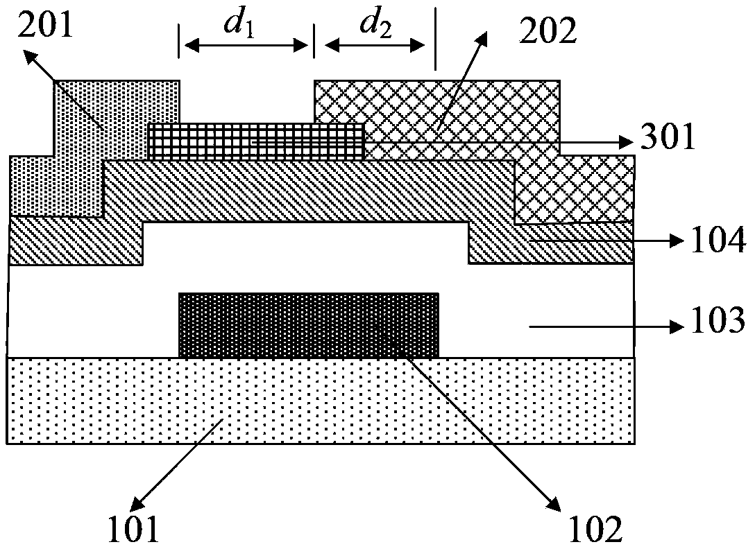
[0036] In order to facilitat...
Embodiment 2
[0050] Such as figure 2 As shown, this embodiment provides an oxide semiconductor thin film transistor, including a substrate 101, a gate electrode 102, an insulating dielectric layer 103, and an oxide semiconductor channel layer 104 sequentially arranged on the substrate 101. The insulating dielectric layer 103 insulates the gate electrode 102 from the oxide semiconductor channel layer 104, the upper surface of the oxide semiconductor channel layer 104 is provided with a drain electrode 201 and a source electrode 202, and the drain electrode 201 and the source electrode The gap between 202 is d 1 , the length of the overlapping region between the source electrode 202 and the gate 102 in the horizontal direction is d 2 The contact between the source electrode 202 and the oxide semiconductor channel layer 104 is a Schottky contact, and the contact between the drain electrode 201 and the oxide semiconductor channel layer 104 is an ohmic contact.
[0051] In order to facilitat...
Embodiment 3
[0065] Such as figure 2 As shown, this embodiment provides an oxide semiconductor thin film transistor, including a substrate 101, a gate electrode 102, an insulating dielectric layer 103, and an oxide semiconductor channel layer 104 sequentially arranged on the substrate 101. The insulating dielectric layer 103 insulates the gate electrode 102 from the oxide semiconductor channel layer 104, the upper surface of the oxide semiconductor channel layer 104 is provided with a drain electrode 201 and a source electrode 202, and the drain electrode 201 and the source electrode The gap between 202 is d 1 , the length of the overlapping region between the source electrode 202 and the gate 102 in the horizontal direction is d 2 The contact between the source electrode 202 and the oxide semiconductor channel layer 104 is a Schottky contact, and the contact between the drain electrode 201 and the oxide semiconductor channel layer 104 is an ohmic contact.
[0066]In order to facilitate...
PUM
 Abstract
Description
Claims
Application Information

