

Heterojunction solar cell and manufacturing method thereof
A solar cell and heterojunction technology, which is applied in the field of solar cells, can solve problems such as unfavorable carrier transport, lower crystal quality, and lower solar cell efficiency, so as to avoid carrier recombination loss and improve photoelectric performance and efficiency , Improve the effect of transportation efficiency
- Summary
- Abstract
- Description
- Claims
- Application Information
AI Technical Summary
Problems solved by technology
Method used
Image

Examples
no. 1 Embodiment
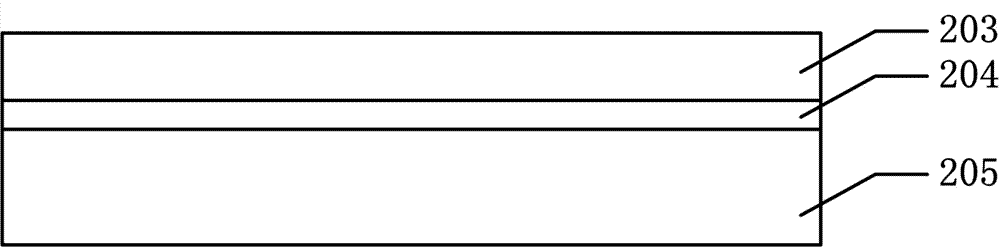
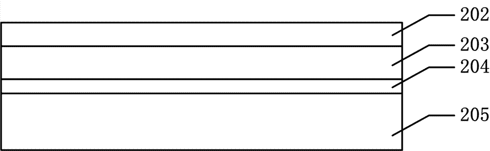
[0028] This specific embodiment provides a heterojunction solar cell with a structure such as Figure 4E As shown, it includes a first film 403 with a first conductivity type, an active region 402 and a second film 401 with a second conductivity type arranged in sequence on the surface of the first film 403, and the first film 403 Between the active region 402 and a contact layer 408 of the first conductivity type that is heterogeneous with the first film 403, the first film 403 and the second film 401 are respectively heterogeneous with the active region 402, and the active Region 402 is a graded layer structure. The contact layer 408 and the active region 402 with the graded layer reduce the barrier height between the first thin film 403 and the active region 402 and between the second thin film 401 and the active region 402. Compared with traditional solar cells, The carrier transport efficiency is improved.
[0029] The above-mentioned first conductivity ty...
no. 2 Embodiment
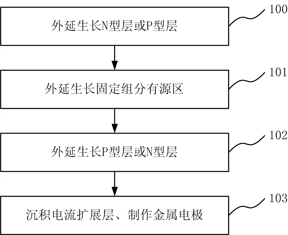
[0043] image 3 Shown is the method flowchart of the second specific embodiment of the method for manufacturing a heterojunction solar cell.
[0044] Figures 4A to 4E Shown is a flow chart of the process steps of the second specific embodiment of the preparation of the heterojunction solar cell.
[0045] This specific embodiment provides a method for preparing a heterojunction solar cell as described in the first specific embodiment, including steps:
[0046] Step 300, growing a contact layer of the same conductivity type as the first thin film on the exposed surface of the first thin film;
[0047] Step 301, epitaxially growing an active region with a graded structure on the exposed surface of the contact layer;
[0048]Step 302 , growing a second thin film layer heterogeneous to that of the active region on the exposed surface of the active region, and the conductivity type of the first thin film is opposite to that of the second thin film.
[0049] As an optiona...
PUM
 Abstract
Description
Claims
Application Information