Base substrate, resonator, oscillator, and electronic device

A technology for base substrates and electronic components, applied in piezoelectric devices/electrostrictive devices, circuits, electrical components, etc., can solve problems such as inability to ensure package sealing and poor wiring tightness

Active Publication Date: 2012-10-17
SEIKO EPSON CORP
View PDF6 Cites 7 Cited by
  • Summary
  • Abstract
  • Description
  • Claims
  • Application Information

AI Technical Summary

Problems solved by technology

[0009] However, in a package with this structure, a portion (intersection) where the bonding material intersects the wiring (the bonding material overlaps the wiring) inevitably occurs.
[0010] Therefore, the packaging of the above-mentioned structure may cause such a new problem: for example, when the bo

Method used


Image

  • Base substrate, resonator, oscillator, and electronic device
  • Base substrate, resonator, oscillator, and electronic device
  • Base substrate, resonator, oscillator, and electronic device

Examples


no. 1 Embodiment approach

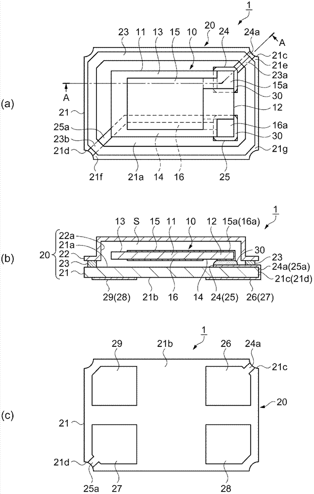
[0043] First, a quartz resonator as an example of a resonator will be described.

[0044] figure 1 It is a schematic diagram showing the schematic structure of the crystal resonator of the first embodiment. figure 1 (a) is a front plan view viewed from the lid side, figure 1 (b) is alongfigure 1 A sectional view of line A-A in (a), figure 1 (c) is a rear plan view seen from the lid side. In the front plan view, the cover portion is omitted. In addition, the dimensional ratios of the respective constituent elements are different from actual ones.

[0045] Such as figure 1 As shown, the crystal vibrator 1 includes a crystal vibrating piece 10 as a vibrating piece, and a package 20 that accommodates the quartz vibrating piece 10 .

[0046] The quartz vibrating piece 10 is an AT-cut shape cut out at a predetermined angle from a quartz rough or the like, and its planar shape is formed into a substantially rectangular shape. The quartz vibrating piece 10 has a vibrating part 1...

Deformed example 1

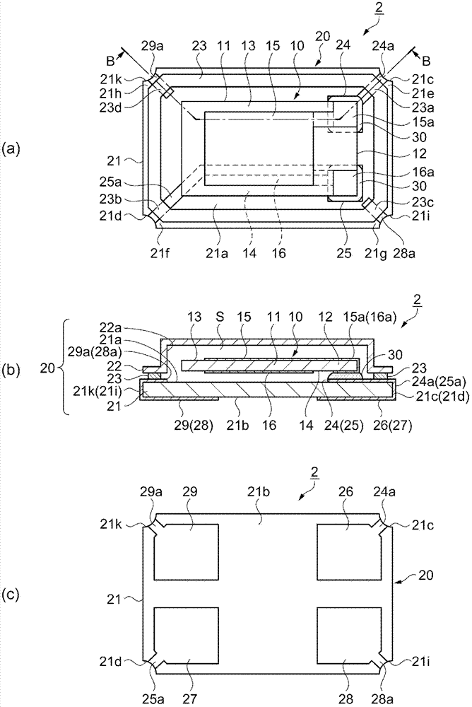
[0089] figure 2 It is a schematic diagram showing a schematic configuration of a crystal resonator in Modification 1. FIG. figure 2 (a) is a front plan view viewed from the lid side, figure 2 (b) is along figure 2 Sectional view of line B-B in (a), figure 2 (c) is a rear plan view seen from the lid side. In the front plan view, the cover portion is omitted. In addition, the dimensional ratios of the respective constituent elements are different from actual ones. In addition, the same code|symbol is attached|subjected to the same part as the said 1st Embodiment, a detailed description is abbreviate|omitted, and it demonstrates centering on the part different from the said 1st Embodiment.

[0090] Such as figure 2 As shown, with regard to the quartz vibrator 2, the wirings 28a, 29a intersect the bonding material 23 at the third corner 21g and the fourth corner 21h located at the other diagonal corner of the one main surface 21a of the base part 21, and the wirings 28a...

Deformed example 2

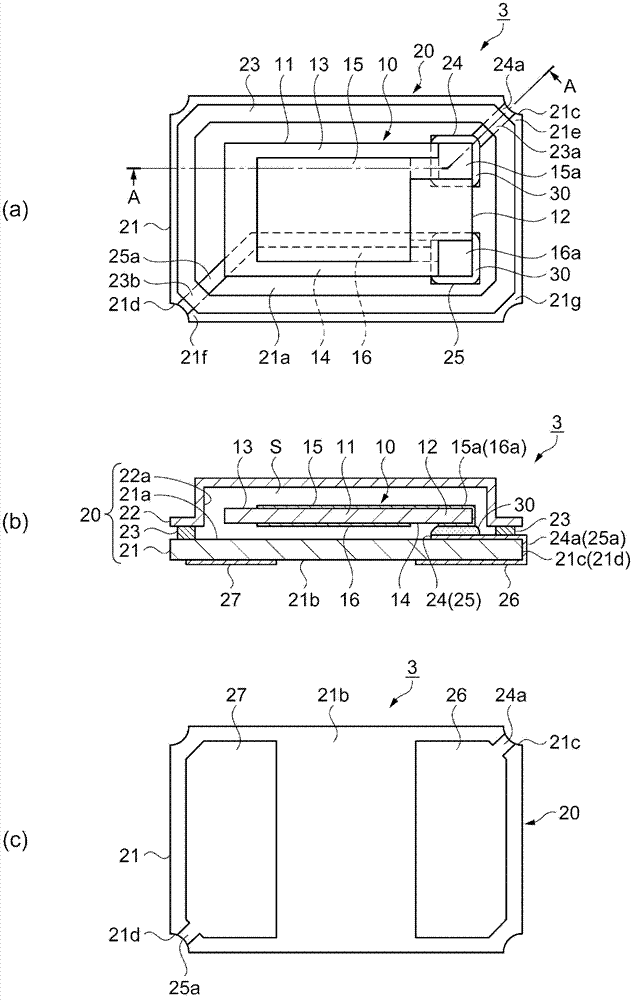
[0099] image 3 It is a schematic diagram showing a schematic configuration of a crystal resonator in Modification 2. FIG. image 3 (a) is a front plan view viewed from the lid side, image 3 (b) is along image 3 A sectional view of line A-A in (a), image 3 (c) is a rear plan view seen from the lid side. In the front plan view, the cover portion is omitted. In addition, the dimensional ratios of the respective constituent elements are different from actual ones. In addition, the same code|symbol is attached|subjected to the same part as the said 1st Embodiment, a detailed description is abbreviate|omitted, and it demonstrates centering on the part different from the said 1st Embodiment.

[0100] Such as image 3 As shown, regarding the crystal vibrator 3, the external electrodes 28, 29 are removed (refer to figure 1 ), and the external electrodes 26, 27 extend to their positions.

[0101] As a result, since the area of ​​the external electrodes 26 and 27 of the base ...


PUM

PropertyMeasurementUnit
Softening pointaaaaaaaaaa

Abstract

The invention provides a base substrate, a resonator, an oscillator, and an electronic device, which guarantees tightness and realizes low cost. A package (20) of a quartz resonator (1) includes a tabular base substrate (21), a base material of which is a single layer, a lid section (22) that has a recess (22a) and covers the base substrate (21), and a bonding material (23) provided over the entire periphery of one principal plane (21a) of the base substrate (21) and including low-melting glass for bonding the base substrate (21) and the lid section (22). Internal electrodes (24, 25) are provided on the one principal plane (21a) of the base substrate (21). External electrodes (26, 27, 28, 29) are provided on the other principal plane (21b) of the base substrate (21). A wire (24a) contains an Ag-Pd alloy having a glass component and crosses the bonding material (23) on the one principal plane (21a).

Description

technical field [0001] The present invention relates to a package, a vibrator including a vibrating piece in the package, an oscillator, and electronic equipment. Background technique [0002] Conventionally, as a package used for piezoelectric devices such as piezoelectric vibrators, semiconductor elements, etc., there is known a package having a structure in which internal electrodes are provided on a flat plate-shaped package base composed of a single layer of ceramic material, and the internal electrodes are connected to the package substrate. The external electrodes on the bottom surface of the package base are connected via conductive lines penetrating the package base (for example, refer to Patent Document 1). [0003] Patent Document 1: Japanese Patent Application Laid-Open No. 9-283650 [0004] The package described above is intended to reduce manufacturing costs, and the package base (hereinafter referred to as "base part") is a single-layer flat plate. [0005] ...

Claims


Application Information

Patent Timeline
IPC IPC(8): H03H9/10H03H9/19
CPCH03H9/19H03H9/10H01L2224/48091H01L2224/48227H03H9/1014H01L2924/00014H01L23/12H10N30/00
Inventor 黑田胜巳
Owner SEIKO EPSON CORP
Why Eureka
Try Eureka