Display device and fabrication method thereof

a technology of a display device and a fabrication method, which is applied in the direction of semiconductor devices, basic electric elements, electrical equipment, etc., can solve the problems of increased man-hours in the fabrication of thin film transistors and the requirement of special equipment for the back-surface exposure step, so as to reduce the amount of fabrication man-hours

Active Publication Date: 2007-05-17
PANASONIC LIQUID CRYSTAL DISPLAY CO LTD +1
View PDF6 Cites 6 Cited by
  • Summary
  • Abstract
  • Description
  • Claims
  • Application Information

AI Technical Summary

Benefits of technology

[0034] In the fabrication method of a display device having such a constitution, the thin film transistor, in forming the first impurity region and the second impurity region in the region defined between the channel region and source / drain region (the third impurity region) of the semiconductor layer, sets the doping energy of impurities different from the conventional doping energy of impurities by making use of the first gate electrode which is formed above the first impurity region thus realizing the formation of the first impurity region and the second impurity region with ion implantation of only one time. Further, in such an operation, the first gate electrode and the second gate electrode which are already formed by patterning are utilized as masks. Accordingly, the fabrication method of the display device of the present invention adopts the constitution which does not use so-called photo masks thus largely reducing the fabricating man-hours.

Problems solved by technology

However, the thin film transistor having the constitution shown in JP-A-2002-190479 has a drawback that man-hours are increased in the fabrication of the thin film transistor.
Further, in the above-mentioned case, a so-called back-surface exposure technique is adopted to suppress the number of photo mask steps and hence, there also arises a drawback that a special apparatus is required for the back-surface exposure step.

Method used


Image

  • Display device and fabrication method thereof
  • Display device and fabrication method thereof
  • Display device and fabrication method thereof

Examples


Embodiment Construction

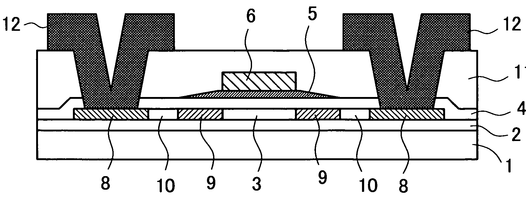
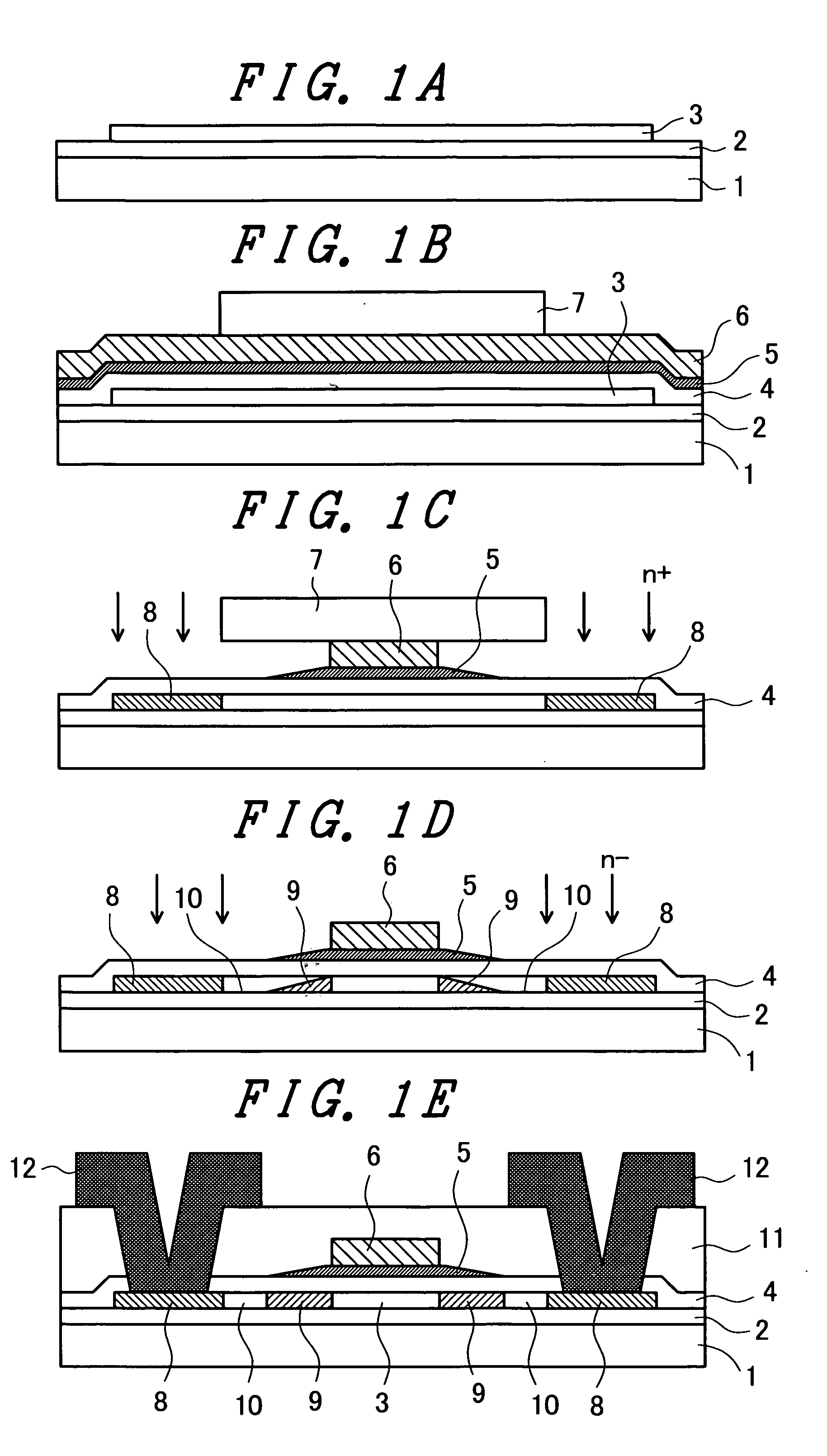
[0039] Embodiments of a fabrication method of a display device according to the present invention are explained hereinafter.

[0040] Here, although the explanation is made hereinafter describes a fabrication method of a thin film transistor which is incorporated into the display device, the fabrication of the thin film transistor should be understood as a part of a series of fabrication steps of the display device.

[0041] That is, the display device includes a substrate which constitutes a display screen, a large number of pixels are arranged on a surface of the substrate in a matrix array, and a mass of these respective pixels constitutes a display part. A drive circuit which drives the respective pixels is provided outside the display part, and groups of pixels each of which is formed of respective pixels arranged in parallel in the row direction, for example, are sequentially selected in the column direction by the drive circuit and, at the same time, video signals are supplied to...


PUM

PropertyMeasurementUnit
sizeaaaaaaaaaa
conductiveaaaaaaaaaa
concentrationaaaaaaaaaa

Abstract

The present invention provides a fabrication method of a display device which aims at the reduction of fabricating man-hours. In a fabrication method of a display device having a thin film transistor in which a gate electrode includes a first gate electrode and a second gate electrode which is overlapped to the first gate electrode and has a size thereof in the channel direction set smaller than the corresponding size of the first gate electrode, the semiconductor layer includes a channel region which is overlapped to the second gate electrode, a first impurity region which is overlapped to the first gate electrode and is formed outside the second gate electrode, a second impurity region which is formed outside the gate electrode, and a third conductive impurity region which is formed outside the gate electrode and the second impurity region, the first impurity region, the second impurity region and the third impurity region are respectively formed of the same conductive type, the impurity concentration of the first impurity region is lower than the impurity concentration of the third impurity region, and the impurity concentration of the second impurity region is lower than the impurity concentration of the first impurity region, impurities are collectively implanted into both of the first and second impurity regions such that the impurities are implanted into the first impurity region by way of the first gate electrode and the impurities are implanted into the second impurity region such that a peak position of the impurity concentration in the depth direction is positioned below the semiconductor layer thus lowering the impurity concentration of the second impurity region than the impurity concentration of the first impurity region.

Description

[0001] The present application claims priority from Japanese application JP2005-332701 filed on Nov. 7, 2005, the content of which is hereby incorporated by reference into this application. BACKGROUND OF THE INVENTION [0002] The present invention relates to a display device, for example, a display device such as a liquid crystal display device or an organic EL display device and a fabrication method thereof. [0003] This type of display device includes a switching element in the inside of each pixel or in the inside of a circuit portion which is provided outside a display portion which is constituted of these pixels for driving respective pixels. [0004] As such a switching element, there has been known a switching element which uses a thin film transistor in which a polycrystalline silicon layer constitutes a semiconductor layer. In this case, usually, the circuit part is formed on the same substrate which is used as a substrate of a display part and, at the same time, the thin film ...

Claims


Application Information

Patent Timeline
Patent Type & Authority Applications(United States)
IPC IPC(8): H01L29/04H01L21/84
CPCH01L29/42384H01L29/4908H01L29/78621H01L29/78696H01L2029/7863
Inventor OUE, EIJIITOGA, TOSHIHIKOKANEKO, TOSHIKISONODA, DAISUKEKURIYAGAWA, TAKESHI
Owner PANASONIC LIQUID CRYSTAL DISPLAY CO LTD
Why Eureka
Try Eureka