High voltage terminal

A terminal, high-voltage technology, applied in electrical components, circuits, semiconductor devices, etc., to reduce costs, shorten processing cycles, and shorten the width of terminals

Inactive Publication Date: 2014-12-24
李思敏
View PDF2 Cites 1 Cited by
  • Summary
  • Abstract
  • Description
  • Claims
  • Application Information

AI Technical Summary

Problems solved by technology

Terminal extensions using junctions, or ITE, can be used with the narrowest terminal widths, however, require a dedicated extra photolithography

Method used


Image

  • High voltage terminal
  • High voltage terminal
  • High voltage terminal

Examples


Embodiment Construction

[0015] The invention will be described in detail below by means of preferred embodiments with reference to the accompanying drawings.

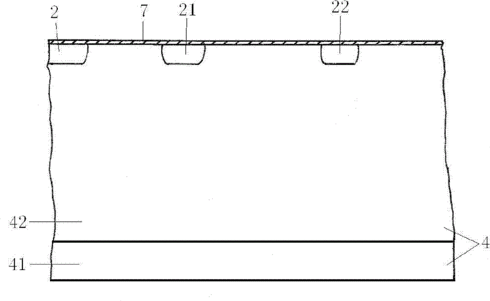
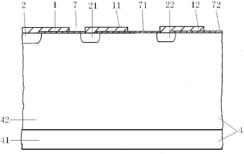
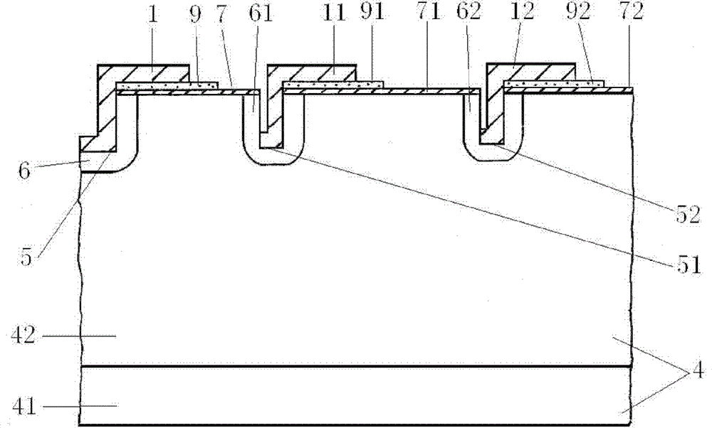
[0016] Among the figure: 1. the aluminum field plate that is connected with the grooved grid region (the prior art is the main junction of the base area): 11. the aluminum field plate that is connected with the first field limiting ring: 12. the second field plate Aluminum field plates connected by rings: 2. P-type base main junction: 21. The first P-type field limiting ring of the prior art high-voltage terminal: 21. The second P-type of the prior art high-voltage terminal Field limiting ring: 4. Silicon substrate: 41. Lower layer of N+ type silicon substrate: 42. Upper layer of N-type silicon substrate: 5. Silicon groove of P+ type groove gate area: 51. The first P+ type groove shape Silicon groove of the field limiting ring: 52. Silicon groove of the second P+ type grooved field limiting ring: 6. P+ type grooved gate area: 61. The first P+ ...


PUM


Abstract

Disclosed is a high voltage terminal. A heavy doping P+ type groove-shaped field limiting ring is arranged on the periphery of an active area of a gate associated transistor of a groove-shaped gate polycrystalline silicon structure, the depth of a groove is in a range from 1micrometers to 6 micrometers, a heavy doping N+ type polycrystalline silicon annular field plate is arranged above the field limiting ring, the upper surface of the polycrystalline silicon field plate is connected with a metal layer AL, and the metal layer AL is connected with the bottom surface of the groove of the P+ type groove-shaped field limiting ring. The high voltage terminal has the advantages that the high voltage terminal is matched with a transistor core process of the gate associated transistor of the groove-shaped gate polycrystalline silicon structure, materials are saved, photoetching times are reduced, the cost is lowered, and the processing cycle is shortened.

Description

technical field [0001] The invention relates to a high-voltage terminal, which belongs to the technical field of silicon semiconductor power devices. Background technique [0002] Tie-gate transistors with groove gate polysilicon structure are a new type of high-voltage power devices. High-voltage power devices are generally terminated using field-limiting rings, field plates, and junction termination extensions (ITE). The college textbook "Power MOSFET and High Voltage Integrated Circuit" (Chen Xingbi Southeast University Press, May 1990) PP 86-120 has a detailed introduction to this. [0003] figure 1 is a structural schematic diagram of a field-limited loop terminal in the prior art, figure 2 It is a structural schematic diagram of a terminal combined with a field plate and a field limiting ring in the prior art. The lower layer 41 of the silicon substrate 4 is N+ type silicon, and the upper layer 42 is N − type silicon. The main base junction 2 and the field limiti...

Claims


Application Information

Patent Timeline
Patent Type & Authority Patents(China)
IPC IPC(8): H01L29/06H01L29/40H01L29/78
Inventor 李思敏
Owner 李思敏
Why Eureka
Try Eureka