Double-sided heterojunction solar cell and preparation method

A solar cell and heterojunction technology, which is applied in the field of solar cells, can solve the problems of large contact interface and the bottleneck of conversion efficiency of heterojunction cells, etc., and achieve the effects of reducing the photosensitive area, reducing the contact area, and reducing shading loss

Active Publication Date: 2014-12-31
TRINA SOLAR CO LTD
View PDF5 Cites 0 Cited by
  • Summary
  • Abstract
  • Description
  • Claims
  • Application Information

AI Technical Summary

Problems solved by technology

[0004] Another major factor affecting heterojunction solar cells is interface state recombination. The emitter layer of a traditional silicon heterojunction solar cell covers the entire area of ​​a single crystal silicon substrate, and the contact interface in the junction region is relatively large. However, the thin film / crystalline The problem of silicon interface contact has always been the bottleneck of the conversion efficiency of heterojunction cells

Method used


Image

  • Double-sided heterojunction solar cell and preparation method
  • Double-sided heterojunction solar cell and preparation method

Examples


Embodiment Construction

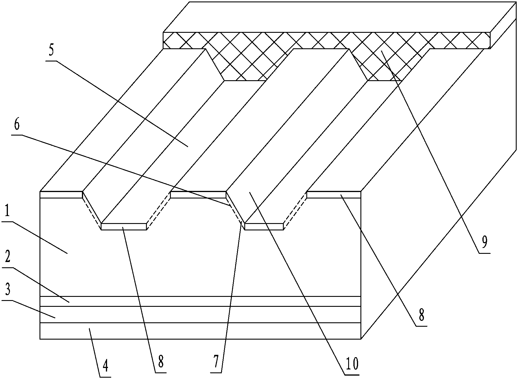
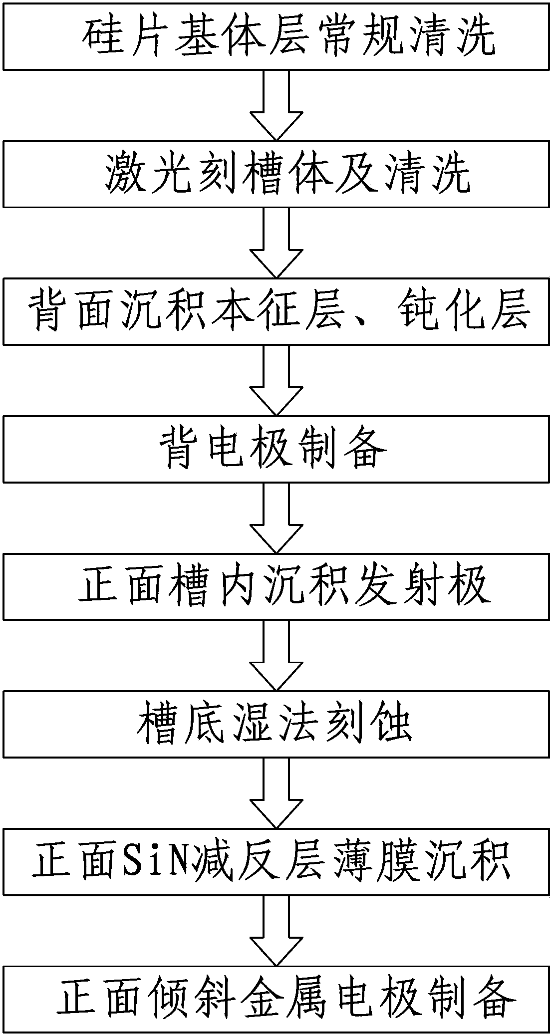
[0024] The present invention will now be further described in conjunction with the accompanying drawings and preferred embodiments. These drawings are all simplified schematic diagrams, which only illustrate the basic structure of the present invention in a schematic manner, so they only show the configurations related to the present invention.

[0025] Such as figure 1 A double-sided heterojunction solar cell shown includes a silicon wafer base layer 1 made of an n-type single crystal silicon wafer. The silicon wafer base layer 1 has a thickness of 200 μm and a resistivity of 5Ω. The silicon wafer base layer 1. The back has an intrinsic layer 2, a heavily doped BSF layer 3 and a back electrode 4 in order from the inside to the outside, wherein the thickness of the intrinsic layer 2 is 5nm, the thickness of the heavily doped BSF layer 3 is 20nm, and the back electrode 4 is selected The metallic aluminum film is deposited with a thickness of 1.5 μm.

[0026] The front side of...


PUM


Abstract

The invention discloses a double-sided heterojunction solar cell and a preparation method. The solar cell comprises a silicon slice base layer; the back surface of the silicon slice base layer is provided with an intrinsic layer, a heavily doped BSF layer and a back electrode from inside to outside in sequence; tilted slots are arranged on the front face of the silicon slice base layer in parallel; intrinsic silicon films and p-type silicon film layers are respectively arranged on the inclined planes of the slots; the p-type silicon film layer is provided with a transparent conductive film used as a positive electrode; the transparent conductive film and the bottom surfaces of the slots are respectively provided with film anti-reflection layers; the surface of the silicon slice base layer is further provided with a silver paste layer which is electrically connected with the transparent conductive film. As the electrode is arranged in a tilting way in the invention, and as the p-type silicon film layers are arranged on the inclined planes of the slots, the p-type silicon film layers are in tilting contact with the electrode; the advantage that the vertical projection area of the inclination planes of the slots is small is fully utilized, thus, the shading loss of the overall solar cell by the positive electrode is reduced, the spectral response of the solar cell is effectively improved and the improvement of the overall performance of the cell is favored.

Description

technical field [0001] The invention relates to the technical field of solar cells, in particular to a double-sided heterojunction solar cell and a preparation method thereof. Background technique [0002] Silicon heterojunction solar cells use amorphous silicon thin films deposited on crystalline silicon substrates as emitters, but doped amorphous silicon emitter thin films can absorb part of the visible light, which affects the effective use of light by the base substrate. It is beneficial to the short-wave response of the cell and limits the conversion efficiency of the solar cell. It can be seen that reducing the light absorption of the emissive layer becomes an effective way to improve the conversion efficiency of the heterojunction solar cell. At present, wide bandgap silicon films are mainly used as the emission layer, but the cost of complex doping process is high, and the electrical properties of wide bandgap doped films cannot be guaranteed. [0003] For heterojun...

Claims


Application Information

Patent Timeline
Patent Type & Authority Patents(China)
IPC IPC(8): H01L31/0747H01L31/0352H01L31/0224H01L31/18
CPCY02E10/50Y02P70/50
Inventor 郭万武
Owner TRINA SOLAR CO LTD
Why Eureka
Try Eureka