A kind of preparation method of graphene/gallium arsenide solar cell

A technology of solar cells and gallium arsenide, applied in the field of solar energy, can solve the problems of increasing the photo-generated carrier recombination center, improving the photoelectric conversion efficiency of gallium arsenide solar cells, large series resistance and recombination current, etc., so as to improve the photoelectric conversion efficiency. , reduce shading loss, improve the effect of filling factor

Active Publication Date: 2018-02-02
INST OF MICROELECTRONICS CHINESE ACAD OF SCI
View PDF4 Cites 0 Cited by
  • Summary
  • Abstract
  • Description
  • Claims
  • Application Information

AI Technical Summary

Problems solved by technology

In the traditional GaAs solar cell manufacturing process, although the heavily doped GaAs cap layer can form a good ohmic contact with the positive electrode, it increases the recombination center of photogenerated carriers, resulting in a large series resistance and In addition, the dense front electrode grid lines will cause a large shading loss, which further restricts the improvement of the photoelectric conversion efficiency of gallium arsenide solar cells

Method used


Image

  • A kind of preparation method of graphene/gallium arsenide solar cell
  • A kind of preparation method of graphene/gallium arsenide solar cell
  • A kind of preparation method of graphene/gallium arsenide solar cell

Examples


preparation example Construction

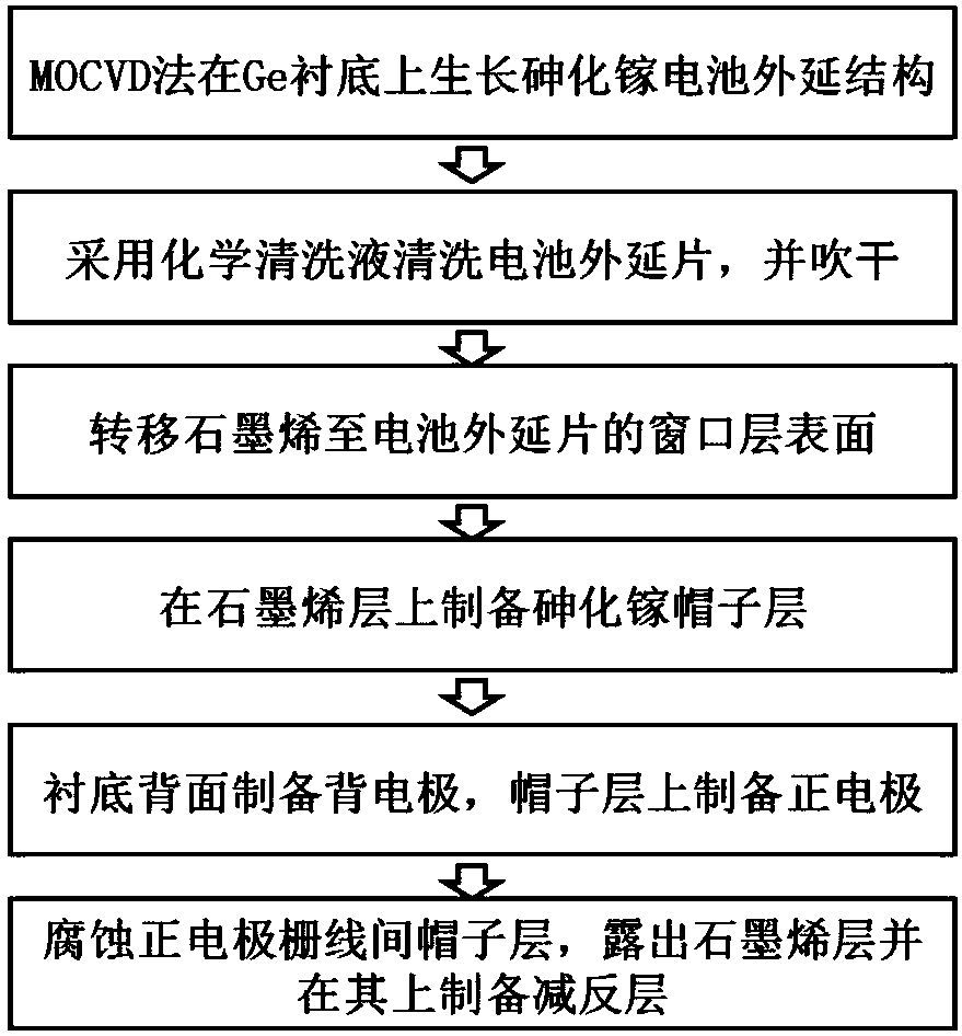
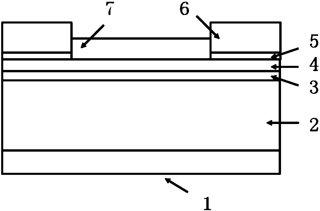
[0024] The invention provides a method for preparing a graphene / gallium arsenide solar cell, comprising the following steps:

[0025] 1) transfer the graphene to the surface of the window layer on the surface of the gallium arsenide epitaxial wafer to form a graphene layer;

[0026] 2) Prepare a heavily doped gallium arsenide cap layer on the surface of the graphene layer;

[0027] 3) preparing a back electrode on the surface of the gallium arsenide epitaxial wafer substrate, and preparing a front electrode on the surface of the heavily doped gallium arsenide cap layer;

[0028] 4) The heavily doped gallium arsenide cap layer between the front electrode grid lines is etched by chemical etching to expose the graphene layer, and an anti-reflection layer is prepared on the surface of the exposed graphene layer.

[0029] In some specific embodiments of the present invention, a cleaning step is also included before step 1). Specifically, the gallium arsenide epitaxial wafer is pla...
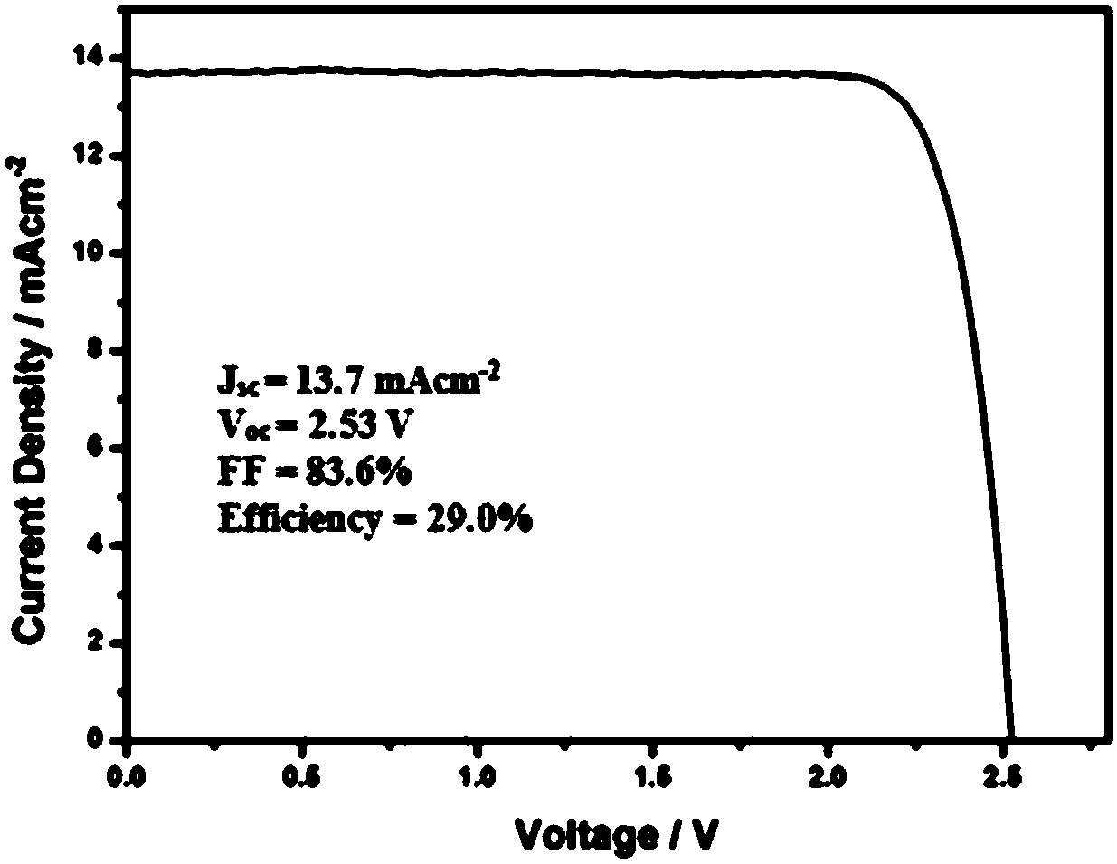
Embodiment 1

[0073] 1) Place the single-junction GaAs cell epitaxial wafer with the structure of GaAs / GaAs in acetone, isopropanol, and absolute ethanol, respectively, and heat it in a 60°C water bath for 15 minutes, then rinse with deionized water for 10 minutes, and then place in HCl:H 2 Soak in the solution of O=1:10 at room temperature for 1min, finally wash with deionized water and blow dry with nitrogen;

[0074] 2) transfer the monolayer graphene to the window layer on the surface of the epitaxial wafer by electrochemical method;

[0075] 3) Depositing a heavily doped gallium arsenide cap layer on the graphene layer by MOCVD;

[0076] 4) Prepare the positive electrode pattern on the surface of the heavily doped gallium arsenide cap layer by photolithography technology, and prepare the alloy back electrode and positive electrode of nickel, germanium and gold by electron beam evaporation method, remove the photoresist and alloy, and then The epitaxial wafer placed in NH 3 ·H 2 O:H...

Embodiment 2

[0085] 1) Place a single-junction GaAs cell epitaxial wafer with a structure of GaAs / Ge in acetone, isopropanol, and absolute ethanol at 50°C for 20 minutes, rinse with deionized water for 10 minutes, and then place in H 2 SO 4 :H 2 o 2 :H 2 Soak in the solution of O=1:8:500 at room temperature for 3min, finally wash with deionized water and blow dry with nitrogen;

[0086] 2) transfer three layers of graphene to the window layer on the surface of the epitaxial wafer by electrochemical method;

[0087] 3) Depositing a heavily doped gallium arsenide cap layer on the graphene layer by MOCVD;

[0088] 4) Prepare the positive electrode pattern on the surface of the heavily doped gallium arsenide cap layer by photolithography, and prepare the alloy back electrode and positive electrode of nickel, germanium, silver, and gold by electron beam evaporation, remove the photoresist and alloy, Then place the epitaxial wafer in C 6 h 8 o 7 :H 2 o 2 :H 2 Erosion 20s in the soluti...


PUM


Abstract

The invention provides a preparing method of a graphene / gallium arsenide solar battery. The preparing method comprises the steps of 1, transferring the graphene to the surface of a window layer of the surface of a gallium arsenide epitaxial wafer to form a graphene layer; 2, preparing a heavy doping gallium arsenide cap layer on the surface of the graphene layer; 3, preparing a rear electrode on the surface of the heavy doping gallium arsenide cap layer, and preparing a front electrode on the heavy doping surface of the gallium arsenide cap layer; 4, adopting a chemical etching method to etch the heavy doping gallium arsenide cap layer among grid lines of the front electrode to expose the graphene layer, and preparing an antireflection layer on the exposed graphene layer. According to the graphene / gallium arsenide solar battery, the graphene layer is adopted as a transparent conducting layer, single or more layer of graphene are transferred to a position between a window layer of a traditional unijunction or multijunction gallium arsenide solar battery and the heavy doping gallium arsenide cap layer through a graphene transferring technology, therefore, transverse transport of photo-generated carriers can be promoted, recombination centers of photo-generated carriers can be reduced, series resistance can be reduced, a fill factor can be improved, and photoelectric conversion efficiency of the solar battery can be improved.

Description

technical field [0001] The invention relates to the technical field of solar energy, in particular to a preparation method of a graphene / gallium arsenide solar cell. Background technique [0002] In recent years, global environmental and energy problems have become increasingly severe, and solar cells, as a renewable green new energy, play a vital role in the sustainable development of human beings. Solar cells are devices that convert light energy into electrical energy by using the photovoltaic effect, and can be mainly divided into silicon-based solar cells and compound semiconductors (such as GaAs, CdTe, CuInSe 2 etc.) two types of solar cells, among which the semiconductor solar cells represented by GaAs-based III-V compounds are widely used in the aerospace field because of their high conversion efficiency, high reliability, long life, small and light weight, etc. favored. [0003] On the one hand, since the discovery of graphene in 2004 by Geim, a professor of physi...

Claims


Application Information

Patent Timeline
Patent Type & Authority Patents(China)
IPC IPC(8): H01L31/0216H01L31/0224H01L31/0304H01L31/18
CPCH01L31/02168H01L31/022466H01L31/0304H01L31/184H01L31/1884Y02E10/544Y02P70/50
Inventor 贾锐桂羊羊孙恒超陶科戴小宛金智刘新宇
Owner INST OF MICROELECTRONICS CHINESE ACAD OF SCI
Why Eureka
Try Eureka