Light-facing surface structure of crystalline silicon heterojunction solar cell

A solar cell and heterojunction technology, applied in circuits, electrical components, photovoltaic power generation, etc., can solve the problems of large lightly doped layers, imperfections, and inability to obtain high quality

Pending Publication Date: 2022-08-09
INST OF ELECTRICAL ENG CHINESE ACAD OF SCI
View PDF0 Cites 0 Cited by
  • Summary
  • Abstract
  • Description
  • Claims
  • Application Information

AI Technical Summary

Problems solved by technology

This cannot be realized in crystalline silicon heterojunction solar cells, because the carrier selective contact layer is generally not a perfe

Method used


Image

  • Light-facing surface structure of crystalline silicon heterojunction solar cell
  • Light-facing surface structure of crystalline silicon heterojunction solar cell
  • Light-facing surface structure of crystalline silicon heterojunction solar cell

Examples


Embodiment 1

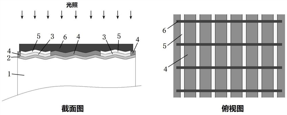
[0053] like figure 1 As shown, a light-facing surface structure of a crystalline silicon heterojunction solar cell includes: a crystalline silicon substrate 1 (N-type doping, resistivity 0.4Ω·cm) and an interface passivation layer 2 ( The thickness is 8nm, and the amorphous silicon interface passivation layer); on the surface of the interface passivation layer 2, a linear selection is performed to set the carrier selective contact surface field layer 3 (the thickness is 15nm, which can be taken out of the crystalline silicon substrate). of electrons of N + The doped nanocrystalline silicon carriers selectively contact the surface field layer, the line width of the line contact region is 300 μm, and the center-to-center spacing between two adjacent line contact regions is 3 mm), and the carrier selective contact surface field is not set The area of ​​the layer 3 is provided with an electrical isolation layer 4 (a silicon oxide electrical isolation layer with a thickness of 100...

Embodiment 2

[0056] like figure 1 As shown, a light-facing surface structure of a crystalline silicon heterojunction solar cell includes: crystalline silicon substrates 1 (P-type doped, surface textured (the textured structure is a randomly distributed pyramid structure) arranged in sequence), The resistivity is 1.5Ω·cm) and the interface passivation layer 2 (thickness is 1nm, silicon oxide interface passivation layer); on the surface of the interface passivation layer 2, a linear selection is performed to set the carrier selective contact surface field Layer 3 (thickness of 100nm, P that can extract holes in the crystalline silicon substrate + The doped polysilicon carriers selectively contact the surface field layer, the line width of the line contact region is 150 μm, and the center-to-center spacing between two adjacent line contact regions is 2 mm), and the carrier selective contact surface field layer is not provided 3 The electrical isolation layer 4 (aluminum oxide electrical isol...

Embodiment 3

[0059] like figure 1 As shown, a light-facing surface structure of a crystalline silicon heterojunction solar cell includes: a crystalline silicon substrate 1 (N-type doped, surface textured (the textured structure is a randomly distributed pyramid structure) arranged in sequence), The resistivity is 4Ω·cm) and the interface passivation layer 2 (thickness is 4nm, amorphous silicon oxide interface passivation layer); on the surface of the interface passivation layer 2, a linear selection is performed to set the carrier selective contact surface Field layer 3 (thickness is 5nm, N which can extract electrons in the crystalline silicon substrate + The doped amorphous silicon carriers selectively contact the surface field layer, the line width of the line contact region is 100 μm, and the center-to-center spacing between two adjacent line contact regions is 1 mm), and the carrier selective contact surface field is not set The area of ​​the layer 3 is provided with an electrical is...


PUM

PropertyMeasurementUnit
Resistivityaaaaaaaaaa
Thicknessaaaaaaaaaa
Line widthaaaaaaaaaa

Abstract

The invention relates to the technical field of crystalline silicon heterojunction solar cells, in particular to a light-facing surface structure of a crystalline silicon heterojunction solar cell. The invention provides a light-facing surface structure of a crystalline silicon heterojunction solar cell. The light-facing surface structure comprises a crystalline silicon substrate and an interface passivation layer which are stacked in sequence, carrying out linear area selection on the surface of the interface passivation layer to set a carrier selective contact surface field layer, and setting an electrical isolation layer in an area without the carrier selective contact surface field layer; the carrier selective contact surface field layer can take out a plurality of carriers in the crystalline silicon substrate; a transparent conductive electrode layer is arranged on the surface of the carrier selective contact surface field layer; grid-shaped metal electrodes are arranged on the surfaces of the electrical isolation layer and the transparent conductive electrode layer; and the grid line orientation of the grid-shaped metal electrode is vertical to the line orientation of the transparent conductive electrode layer. The light-facing surface structure of the crystalline silicon heterojunction solar cell can well improve the short-circuit current density of the crystalline silicon heterojunction solar cell.

Description

technical field [0001] The invention relates to the technical field of crystalline silicon heterojunction solar cells, in particular to a light-facing surface structure of a crystalline silicon heterojunction solar cell. Background technique [0002] Solar photovoltaic power generation is a type of renewable energy utilization with great potential, which has attracted much attention around the world. The core device of photovoltaic power generation is the solar cell, which converts solar energy into electrical energy through the semiconductor photovoltaic effect. At present, the solar cell industry is still dominated by crystalline silicon solar cells, which have long accounted for more than 90% of the world solar cell market share. However, the cost of photovoltaic power generation still needs to fall. The photovoltaic market has a growing demand for high-efficiency crystalline silicon solar cells. [0003] Crystalline silicon heterojunction solar cells have attracted ma...

Claims


Application Information

Patent Timeline
IPC IPC(8): H01L31/0216H01L31/0224
CPCH01L31/02167H01L31/022433H01L31/022466Y02P70/50
Inventor 赵雷王文静
Owner INST OF ELECTRICAL ENG CHINESE ACAD OF SCI
Why Eureka
Try Eureka