Light spot suppression method in bright field defect scanning

A defect scanning and spot technology, which is applied in the field of spot suppression, can solve the problems of affecting the collection of reflected light, unpredictable spot shape, and reducing scanning sensitivity, etc., to achieve the effects of ensuring scanning sensitivity, suppressing impact, and improving scanning quality

Active Publication Date: 2012-11-07
SHANGHAI HUALI MICROELECTRONICS CORP
View PDF5 Cites 3 Cited by
  • Summary
  • Abstract
  • Description
  • Claims
  • Application Information

AI Technical Summary

Problems solved by technology

[0003] During the production process, the pattern on the surface of the semiconductor device will constantly change its shape with different manufacturing processes, and the problem of spot suppression will appear under the special influence of some surface patterns; figure 1 It is a schematic diagram of light spots formed during defect inspection in the background technology of the present invention, such as figure 1 As shown, because part of the pattern 11 on the surface of the chip 1 reflects the incident light of the machine, it forms regular light wave superposition 12 to form a light spot 13, which affects the normal collection of reflected light and reduces the scanning sensitivity.
[0004] At present, the industry is passively making a series of spot blocking layers for the spot problem, that is, analyzing the possible spot shape in advance, then making the corresponding spot blocking, and finally applying it in production. Although this method can be good Suppress some types of light spots, but with the continuous development of semiconductor size and technology, the shape of possible light spots is unpredictable. Therefore, it is urgent to design and manufacture a new light spot analysis and blocking system for bright-field semiconductor defect scanning machines. need

Method used


Image

  • Light spot suppression method in bright field defect scanning
  • Light spot suppression method in bright field defect scanning
  • Light spot suppression method in bright field defect scanning

Examples


Embodiment Construction

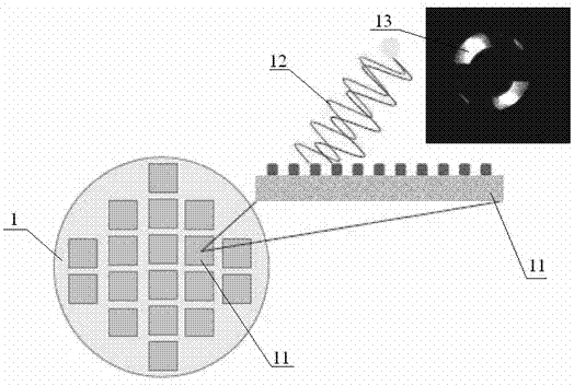
[0020] The specific embodiment of the present invention will be further described below in conjunction with accompanying drawing:

[0021] Figure 2-4 It is a schematic flowchart structure diagram of an embodiment of a method for suppressing light spots in bright field defect scanning according to the present invention.

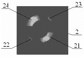
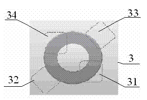
[0022] Such as Figure 2-4 As shown, first, a semiconductor device is prepared, and when the defect scanning process is performed on it, the light spot analysis system (lobes collection) is used to collect and analyze the information of the light spot generated by the semiconductor device on the bright field defect detection machine, Obtaining the shape and position of the light spots that can be formed on the surface of the semiconductor device; then, using a light spot pattern conversion system (lobes image mode) to convert the information of the collected light spots into a light spot pattern 2, wherein the light spot pattern 2 includes the first light sp...


PUM


Abstract

The invention relates to the field of manufacturing of semiconductors, and in particular relates to a light spot suppression method in bright field defect scanning. The light spot suppression method in bright field defect scanning comprises the following steps of: collecting and analyzing light spots generated by a semiconductor device subjected to defect scanning in real time, timely converting the real-time light spot information into a light spot graph, manufacturing a light spot blocking plate with a matched shape according to the light spot graph, and performing a defect detection process according to the light spot blocking plate. Therefore, the influence of the unexpected light spot graph on the process progress can be effectively avoided, the influence of the light spots on the defect detection process is effectively suppressed, and the scanning quality is greatly improved, so that the scanning sensitivity of a cabinet is guaranteed.

Description

technical field [0001] The invention relates to the field of semiconductor manufacturing, in particular to a spot suppression method in bright field defect scanning. Background technique [0002] With the development of integrated circuit technology and the continuous shrinking of critical dimensions, factories need to introduce more advanced and more expensive defect detection equipment to meet the requirements for quality monitoring of online process steps. Among them, bright field defect detection is the most widely used and highly sensitive type of machine. [0003] During the production process, the pattern on the surface of the semiconductor device will constantly change its shape with different manufacturing processes, and the problem of spot suppression will appear under the special influence of some surface patterns; figure 1 It is a schematic diagram of light spots formed during defect inspection in the background technology of the present invention, such as figu...

Claims


Application Information

Patent Timeline
Patent Type & Authority Applications(China)
IPC IPC(8): H01L21/66
Inventor 王洲男龙吟倪棋梁陈宏璘郭明升
Owner SHANGHAI HUALI MICROELECTRONICS CORP
Why Eureka
Try Eureka