Supercharge Your Innovation With Domain-Expert AI Agents!

Nitride read only memory (NROM) structure device with low operating voltage

A low operating voltage, device technology, applied in the field of NROM structure devices, can solve the problems of high programming voltage, unit misprogramming, unfavorable memory chip density, etc.

Active Publication Date: 2015-04-08
SHANGHAI HUALI MICROELECTRONICS CORP
View PDF4 Cites 0 Cited by
  • Summary
  • Abstract
  • Description
  • Claims
  • Application Information

AI Technical Summary

Problems solved by technology

(c) High programming voltage is not conducive to the improvement of memory chip density
(d) High operating voltage will affect the shrinkage of the core memory array (cross-coupling between polysilicon word lines, leading to misprogramming of cells)

Method used


Image

  • Nitride read only memory (NROM) structure device with low operating voltage
  • Nitride read only memory (NROM) structure device with low operating voltage
  • Nitride read only memory (NROM) structure device with low operating voltage

Examples


Embodiment 1

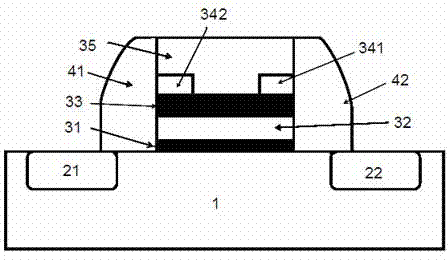
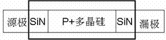
[0023] First prepare the P-type silicon substrate 1, firstly prepare a layer of 3.5nm bottom silicon oxide layer 31 on it, and then prepare a charge-storage silicon nitride layer 32 (N1) with a thickness of about 7nm for storing charges thereon. A blocking silicon oxide layer 33 (O2) of 5 nm thick is then prepared thereon. A silicon nitride layer 34 is deposited thereon, and the middle silicon nitride 34 is removed, and the ratio of the silicon nitride 341 and 342 at both ends and the middle area is controlled at 1:3:1. Then, P-type polysilicon 35 is deposited by an in-situ deposition method, and redundant polysilicon 35 is removed by etching. Finally, sidewalls 41, 42 and source and drain electrodes 21, 22 are formed, thereby forming figure 1 The structure diagram, figure 2 yes figure 1 top view diagram.

Embodiment 2

[0025] First prepare the P-type silicon substrate 1, first prepare a layer of 3.5nm bottom silicon oxide layer 31 on it, and then prepare a charge-storage silicon nitride layer 32 (N1) with a thickness of about 7nm for storing charges on it. . A blocking silicon oxide layer 33 (O2) of about 5 nm thickness is then prepared thereon. P-type polysilicon 35 is deposited thereon, and the polysilicon at both ends is removed, and the ratio between the area at the two ends removed by etching and the remaining area is controlled at 1:3:1. Finally, silicon nitride 341, 342 is deposited, excess silicon nitride is removed, and then sidewalls 41, 42 and source and drain electrodes 21, 22 are formed, so as to form figure 1 The structure diagram, figure 2 yes figure 1 top view diagram.

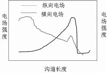
[0026] image 3 It is a schematic diagram of the relationship between the lateral electric field along the channel and the longitudinal electric field of the vertical channel and the channel length of t...


PUM

PropertyMeasurementUnit
thicknessaaaaaaaaaa
thicknessaaaaaaaaaa
thicknessaaaaaaaaaa

Abstract

The invention provides a nitride read only memory (NROM) structure device with a low operating voltage and a preparation method thereof. A layer with a silicon nitride layer and P+ polycrystalline silicon is inserted between a blocking oxidation silicon layer and a polycrystalline silicon gate, wherein the silicon nitride layer and the P+ polycrystalline silicon are crossed transversely. Speeds of electrons in a channel are adjusted by using difference of regional threshold voltages under a gate voltage, so that the electrons have a large speed before reaching a drain terminal or a source terminal (not at a junction of the source or drain terminal and a substrate), in such a way, more electrons are injected into the charge storage silicon nitride layer, and are not easily collected by a high electric field of the source or drain terminal. The programming efficiency is improved, and the programming voltage is reduced, therefore, influences of a high operating voltage on the performance and the reliability of the device are reduced.

Description

technical field [0001] The invention relates to the technical field of semiconductor microelectronics, in particular to an NROM structure device with low operating voltage. Background technique [0002] NROM (nitride based read-only memory) technology has become a strong competitor of the next generation of non-volatile memory due to its ability to provide higher storage density and fast low-voltage programming. NROM has the same simple structure as SONOS devices, is compatible with standard CMOS manufacturing processes, and can use a thicker bottom oxide layer in the accumulation of gate dielectrics, which can improve the retention time of stored electrons and reduce the disturbance of read operations . NROM uses ONO gate dielectric stack to store information, which is different from SONOS devices that use FN tunneling or direct tunneling to write and erase. NROM uses channel hot electrons (the electrons injected into the channel from the source end are accelerated under ...

Claims


Application Information

Patent Timeline
Patent Type & Authority Patents(China)
IPC IPC(8): H01L29/423H01L27/112H01L21/28H01L21/8246
Inventor 田志顾经纶
Owner SHANGHAI HUALI MICROELECTRONICS CORP
Features
  • R&D
  • Intellectual Property
  • Life Sciences
  • Materials
  • Tech Scout
  • Unparalleled Data Quality
  • Higher Quality Content
  • 60% Fewer Hallucinations
Learn More