Unlock instant, AI-driven research and patent intelligence for your innovation.

Low-power-consumption drive circuit

A drive circuit, low power consumption technology, applied in the field of low power drive circuit, can solve the problem of large dynamic power consumption and achieve the effect of reducing power consumption

Active Publication Date: 2015-04-15
BRITE SEMICON SHANGHAI CORP
View PDF4 Cites 0 Cited by
  • Summary
  • Abstract
  • Description
  • Claims
  • Application Information

AI Technical Summary

Problems solved by technology

[0010] It can be seen that the driving circuit with SR control in the prior art has a dynamic current in which the PMOS transistor and the NMOS transistor are turned on at the same time, and the dynamic power consumption is relatively large.

Method used


Image

  • Low-power-consumption drive circuit
  • Low-power-consumption drive circuit
  • Low-power-consumption drive circuit

Examples


Embodiment Construction

[0020] The present invention will be described in detail below in conjunction with the accompanying drawings.

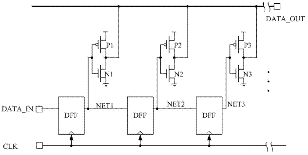
[0021] image 3 It is a block structure diagram of the low power consumption drive circuit in one embodiment of the present invention. Such as image 3 As shown, the low power consumption driving circuit includes a control circuit 100 and a driving stage circuit 200 . The drive stage circuit has more than 200 drive stages, and each drive stage includes a first drive switch (P1, P2 or P3, which can also be called a first drive transistor) and a second drive switch (N1, N2 or N3, It can also be referred to as the first drive tube), the first drive switch is turned on or off under the drive of the first drive signal (NETP1, NETP2 or NETP3), and the second drive switch is turned on or off under the drive of the second drive signal (NETN1, NETN2 or NETN3) is turned on or off. image 3 Three driver stages are shown in , in other embodiments there may be 2, 4 or other n...


PUM


Abstract

The invention discloses a low-power-consumption drive circuit which comprises a drive-stage circuit and a control circuit. The drive-stage circuit comprises a plurality of drive stages, and each drive stage comprises a first drive switch and a second drive switch, wherein the first drive switch is driven by first drive signals, and the second drive switch is driven by second drive signals. The control circuit is used for generating the first drive signals for the first drive switch of each drive stage based on data signals and generating the second drive signals for the second drive switch of each drive stage, and under drive of the first drive signals and the second drive signals, the second drive switch of each drive stage is off before on of the first drive switch of each drive stage, and the first drive switch of each drive stage is off before on of second drive switch of each drive stage. The first drive switches and the corresponding second drive switches are not on simultaneously, so that dynamic power consumption can be reduced.

Description

technical field [0001] The invention relates to a high-speed interface sending part and a high-power output circuit, in particular to a low-power drive circuit with SR (Slew Rate, voltage conversion rate, SR for short) control. Background technique [0002] SR (Slew Rate) is the voltage conversion rate, referred to as the slew rate. Its definition is the amplitude of the voltage increase in 1 microsecond or 1 nanosecond. Intuitively speaking, it is the time required for the square wave voltage to rise from the valley to the peak. The unit is usually V / s, V / ms, V / μs And V / ns four. The voltage slew rate can be measured with an oscilloscope. If the voltage conversion rate is not high, it cannot keep up with the signal accurately and timely when the signal comes, and the amplifier can only keep up with half or less of the original signal level after the signal disappears, making the signal amplitude smaller than the signal, and the analysis ability is also poor. . [0003] C...

Claims


Application Information

Patent Timeline
Patent Type & Authority Patents(China)
IPC IPC(8): H03K19/094H03K17/28
Inventor 王汉祥向涛陆竞虞
Owner BRITE SEMICON SHANGHAI CORP