Glass composition for semiconductor junction protection, production method for semiconductor device, and semiconductor device

A manufacturing method and semiconductor technology, applied in the direction of semiconductor/solid-state device manufacturing, semiconductor devices, semiconductor/solid-state device components, etc., to achieve the effect of high withstand voltage

Active Publication Date: 2012-11-14
SHINDENGEN ELECTRIC MFG CO LTD
View PDF7 Cites 8 Cited by
  • Summary
  • Abstract
  • Description
  • Claims
  • Application Information

AI Technical Summary

Problems solved by technology

[0027] However, the use of "glass materials mainly composed of lead silicate" may be banned in the future because "glass materials mainly composed of lead silicate" contain lead, which has a large environmental load.

Method used


Image

  • Glass composition for semiconductor junction protection, production method for semiconductor device, and semiconductor device
  • Glass composition for semiconductor junction protection, production method for semiconductor device, and semiconductor device
  • Glass composition for semiconductor junction protection, production method for semiconductor device, and semiconductor device

Examples


Embodiment approach 1

[0059] Embodiment 1 is an embodiment related to the glass composition for semiconductor junction protection.

[0060] The glass composition for protecting a semiconductor junction according to Embodiment 1, containing at least SiO 2 、Al 2 o 3 , ZnO, CaO, 3mol% to 10mol% of B 2 o 3 , and substantially does not contain Pb, P, As, Sb, Li, Na, K.

[0061] Specifically, SiO 2 The content of Al is in the range of 32mol%~48mol% (such as 40mol%), Al 2 o 3 The content of ZnO is in the range of 9mol% to 13mol% (such as 11mol%), the content of ZnO is in the range of 18mol% to 28mol% (such as 23mol%), and the content of CaO is in the range of 15mol% to 23mol%. (eg 19mol%), B 2 o 3 The content of the compound is in the range of 3 mol% to 10 mol% (for example, 7 mol%).

[0062] As can be seen from the embodiments described later, the glass composition for protecting a semiconductor junction according to Embodiment 1 uses a glass material that does not contain lead, and can produce...

Embodiment approach 2

[0070] Embodiment 2 is an embodiment related to a manufacturing method of a semiconductor device.

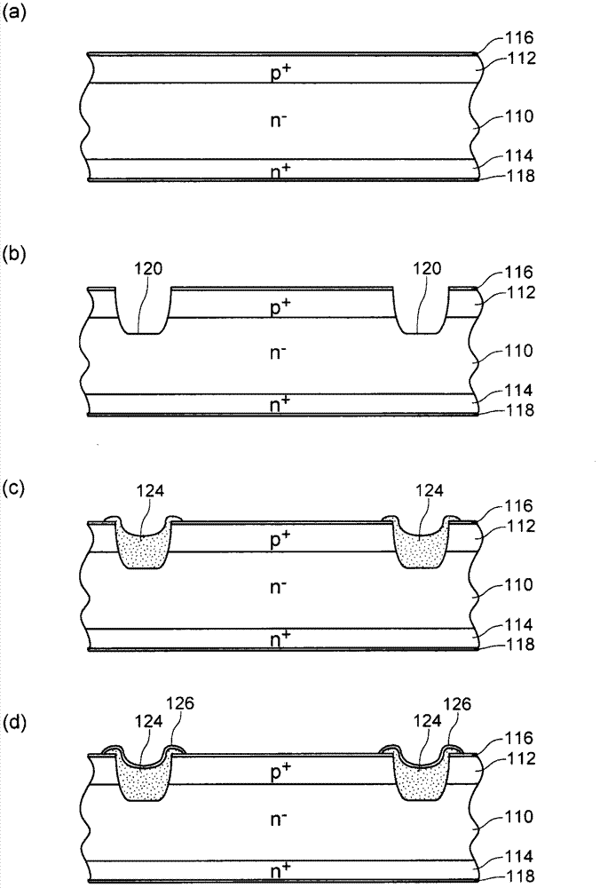
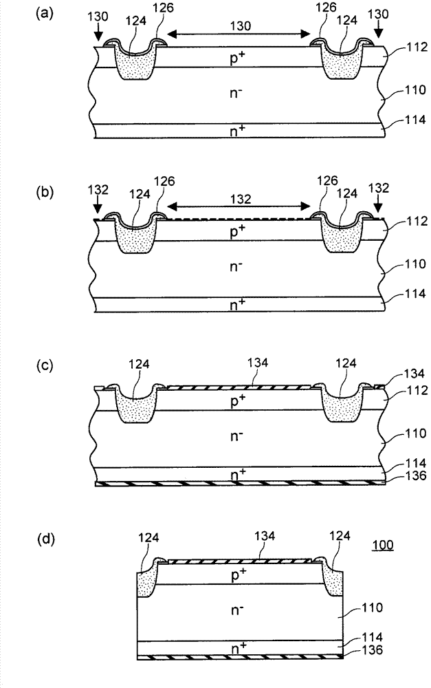
[0071] The method of manufacturing a semiconductor device according to Embodiment 2 is the manufacture of a semiconductor device including, in order, a first step of preparing a semiconductor element having a pn junction exposed portion where the pn junction is exposed, and a second step of forming a glass layer covering the pn junction exposed portion. method. In addition, in the second step, at least SiO is used 2 、Al 2 o 3 , ZnO, CaO, 3mol% to 10mol% of B 2 o 3 , and substantially free of Pb, P, As, Sb, Li, Na, and K for protecting a semiconductor junction (the glass composition for protecting a semiconductor junction according to the first embodiment) forms a glass layer. The first step includes the step of preparing a semiconductor base having a pn junction parallel to the main surface, and forming a groove in the depth of the pn junction from the surface on one side o...

Embodiment approach 3

[0092] Embodiment 3 is an embodiment related to a manufacturing method of a semiconductor device.

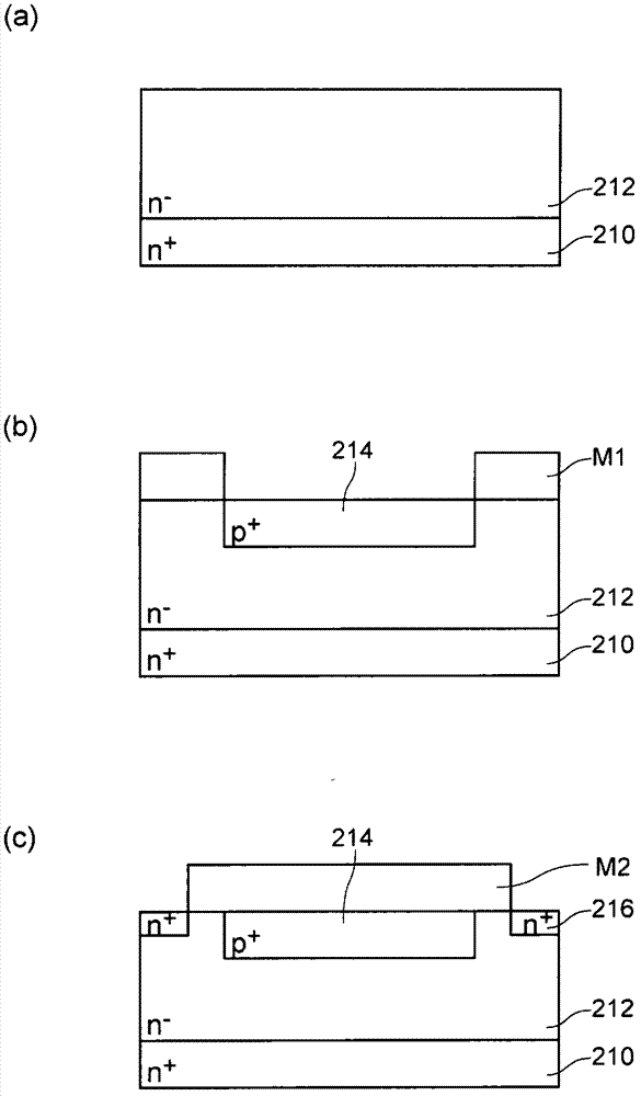
[0093] The method of manufacturing a semiconductor device according to Embodiment 3, similarly to the method of manufacturing a semiconductor device according to Embodiment 2, sequentially includes a first step of preparing a semiconductor element having a pn junction exposed portion where the pn junction is exposed, and forming a step covering the pn junction exposed portion. The second process of the glass layer. Furthermore, in the second step, using at least SiO 2 、Al 2 o 3 , ZnO, CaO, 3mol% to 10mol% of B 2 o 3 , and substantially free of Pb, P, As, Sb, Li, Na, and K for protecting a semiconductor junction (the glass composition for protecting a semiconductor junction according to the first embodiment) forms the glass layer. However, unlike the semiconductor device manufacturing method of Embodiment 2, the first step includes forming a pn junction exposed portion on th...


PUM


Abstract

A glass composition for semiconductor junction protection, characterized by including at least SiO2, Al2O3, ZnO, CaO, and 3-10 mol% of B2O3 and by substantially not including Pb, P, As, Sb, Li, Na, or K. It is desirable that the SiO2 content is within the range of 32-48 mol%, the Al2O3 content is within the range of 9-13 mol%, the ZnO content is within the range of 18-28 mol%, the CaO content is within the range of 15-23 mol%, and the B2O3 content is within the range of 3-10 mol%. Production of a semiconductor device having a high pressure-resistance similar to conventional "glass having lead silicate as the main component thereof" and using a glass material not containing lead is possible using this glass composition for semiconductor junction protection.

Description

technical field [0001] The present invention relates to a glass composition for semiconductor joint protection, a semiconductor device and a manufacturing method thereof. Background technique [0002] Conventionally, there is a semiconductor device manufacturing method in which a passivation glass layer is formed to cover the pn junction exposed part in the manufacturing process of the mesa semiconductor device (for example, refer to Patent Document 1). [0003] Figure 6 and Figure 7 It is an explanatory diagram showing a conventional method of manufacturing a semiconductor device. Figure 6 (a)~ Figure 6 (d) and Figure 7 (a)~ Figure 7 (d) is a diagram of each process. [0004] Such as Figure 6 and Figure 7 As shown, the conventional semiconductor device manufacturing method sequentially includes "semiconductor base formation process", "groove formation process", "glass layer formation process", "photoresist formation process", "oxide film removal process", " rou...

Claims


Application Information

Patent Timeline
Patent Type & Authority Applications(China)
IPC IPC(8): C03C3/066C03C3/093H01L23/29H01L21/56
CPCH01L29/8613H01L2924/0002H01L23/3178C03C8/04C03C3/093H01L23/291C03C3/066H01L29/0661H01L29/8611H01L21/02123C03C8/24H01L21/76232H01L2924/00H01L21/02172H01L21/022H01L21/02318H01L23/564
Inventor 小笠原淳伊藤一彦伊东浩二
Owner SHINDENGEN ELECTRIC MFG CO LTD
Why Eureka
Try Eureka