Display device
A technology for display devices and display areas, applied in identification devices, nonlinear optics, instruments, etc., can solve problems such as insufficient adhesion of sealing materials and alignment films, and inability to completely seal
- Summary
- Abstract
- Description
- Claims
- Application Information
AI Technical Summary
Problems solved by technology
Method used
Image
Examples
Embodiment approach 1
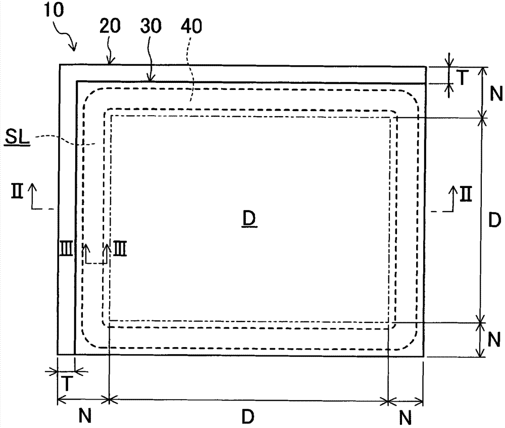
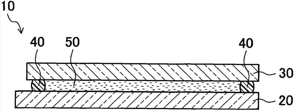
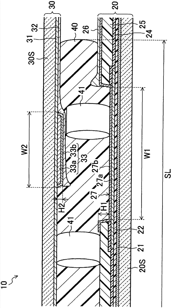
[0090] figure 1 and 2 An overall schematic diagram of the liquid crystal display device 10 according to Embodiment 1 is shown. in addition, image 3 An enlarged cross-sectional view showing the vicinity of the sealing region SL of the liquid crystal display device 10 is shown. and, Figure 4 and 5 The top views of the array substrate 20 and the opposite substrate 30 are shown respectively.
[0091] The liquid crystal display device 10 includes an array substrate 20 (first substrate) and an opposing substrate 30 (second substrate) arranged to face each other. On the substrate main body 20S of the array substrate 20, the first metal (first wiring) including the gate line 21, the gate insulating film 22, and the source line 23 (refer to Figure 6 ) second metal (second wiring); passivation film 24; planarization film 25; third metal including pixel electrodes (not shown); The detailed configuration of the array substrate 20 will be described later. In addition, on the su...
Deformed example 1~3
[0125] In Embodiment 1, it was explained that the grooves 27 are provided in double, and only the groove base metal 27a corresponding to the outermost groove 27 is connected to the transmission pad 28, and the groove base metal 27a of the lower layer of the groove 27 on the inner peripheral side is not formed. The floating state is electrically connected to other wiring, but in the case where the grooves 27 are provided in multiple rows, each groove base metal 27 corresponding to all the grooves 27 may be connected to the transmission pad 28, and conversely, all the grooves may be connected to each other. Base metal 27a is in a suspended state.
[0126] For example, as Modification 1 Figure 12 and 13 As shown, the transfer pad lead-out line 28a may be formed so as to extend to the vicinity of the lower layer of the inner groove 27, and the transfer pad lead-out line 28a may be in contact with the groove base metal 27a of the lower layer of the outer groove 27 through the tra...
Deformed example 4
[0129] In Embodiment 1, the transmission pad 28 is provided with a common potential by the transmission bus line (not shown) provided on the outer periphery thereof, but the transmission bus line may not be provided on the outer periphery of the transmission pad 28, and as in Modification 4, a common potential may be provided. Figure 18 As shown, the groove base metal 27a is made to function as a transmission bus. In this case, the groove base metal 27a is connected to an external connection terminal (not shown) by the common potential input line 28d, and is electrically connected to the transfer pads 28 by the transfer pad lead-out lines 28a. Also, the common potential supplied from the external connection terminal is transmitted to the transfer pad 28 through the trench base metal 27 a. Since the function of the transmission bus is given to the groove base metal 27a, it is possible to omit providing the transmission bus independently on the outer periphery of the transmissi...
PUM
 Abstract
Description
Claims
Application Information


