

Microfluidic chip allowing different cell-density arrangement and use thereof
A microfluidic chip and cell technology, applied in the field of combining microstructure technology and microbiology devices
- Summary
- Abstract
- Description
- Claims
- Application Information
AI Technical Summary
Problems solved by technology
Method used
Image

Examples
Embodiment 1
[0031] Example 1: Preparation of microfluidic chip
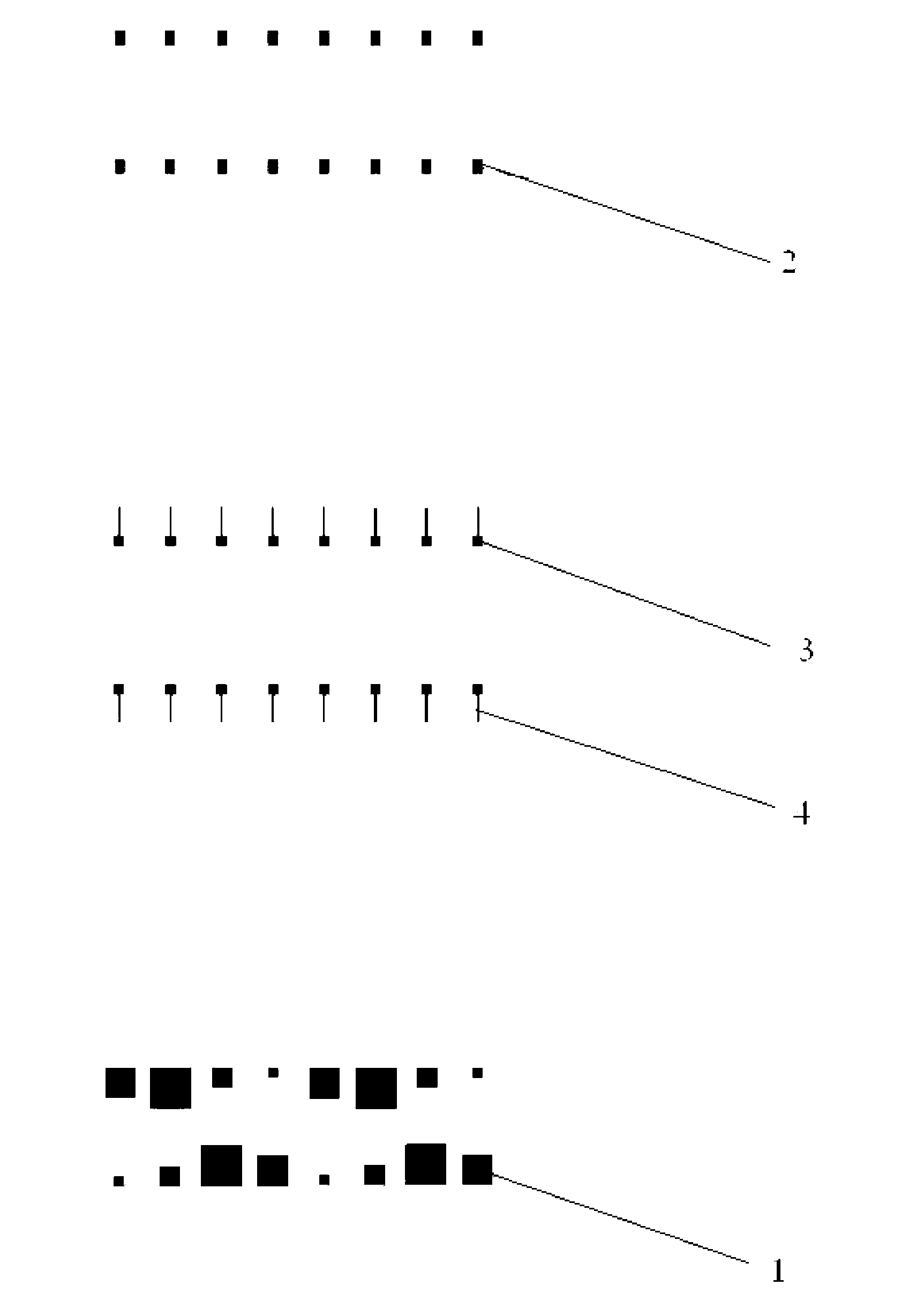
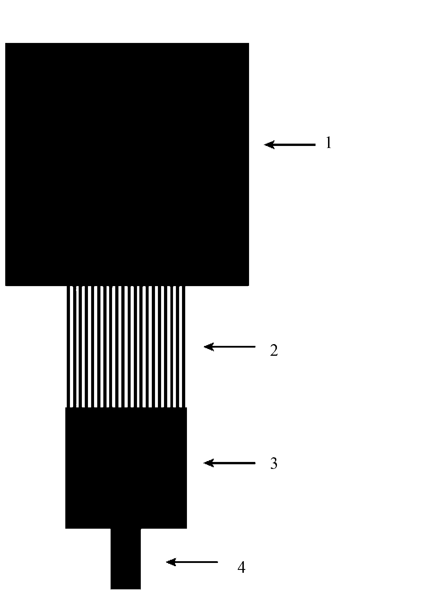
[0032] 1) Draw with L-Edit, make such as figure 1 Graphics, printed on plastic film or optical mask, as exposure mask. The design includes a three-layer structure, which are the cell arrangement chamber 3, the connecting channel 4, the liquid absorption chamber 1, and the fence channel 2 connecting the cell arrangement chamber 3 and the liquid absorption chamber 1 but blocking the passage of cells. The liquid absorption chamber 1, the cell arrangement chamber 3 and the connecting channel 4 are printed on the plastic film, and the fence channel 2 is printed on the optical mask.
[0033] 2) Use the mask pattern obtained in step 1) to prepare a photoresist mold on the silicon wafer through multi-layer alignment sleeve, in which the layer height of the cell arrangement chamber is 20 μm, and the height of the liquid absorption chamber layer is 70 μm. The height of the barrier channel layer is 5 μm. After the overlay is complete...
Embodiment 2
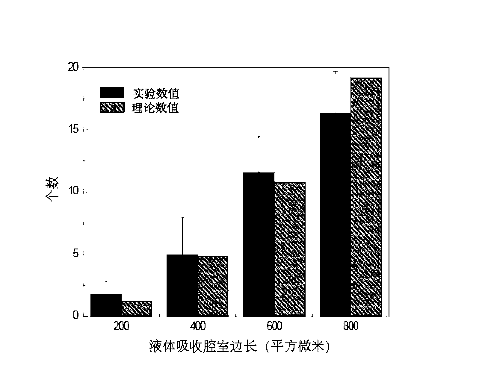
[0036] A microfluidic chip was prepared by the same steps as in Example 1, and each chip included 100 independent cell density arrangement units. Cell arrangement chamber area of 200 × 200 μm constant for all independent units 2 A square whose height is 10 μm, while the area of the liquid-absorbing chamber contains 200 × 200 μm 2 , 200×400μm 2 , 200×600μm 2 , 200×800μm 2In four cases, the height is 20 μm. The barrier channel consists of 20 thin channels with a length of 200 μm, a width of 5 μm, and a height of 10 μm.
[0037] After the mold is prepared, use 3mm thick PDMS (A:B=10:1) to replicate the pattern, cure at 75°C for 30 minutes, cut out the patterned PDMS, and naturally adhere to the petri dish. The chip was irradiated under ultraviolet light for 12h, ready for use.
Embodiment 3
[0039] A microfluidic chip was prepared by the same steps as in Example 1, and each chip included 20 independent cell density arrangement units. The cell arrangement chamber area of each unit includes 100×200μm 2 , 200×200μm 2 , 200×300μm 2 There are 5 chambers for cells of different areas arranged in a square and a rectangle. The area of the liquid absorption chamber is 200×200 μm 2 , the height of which is 20 μm. The barrier channel consists of 20 thin channels with a length of 200 μm, a width of 10 μm, and a height of 5 μm.
[0040] After the mold is prepared, use 6mm thick PDMS (A:B=10:1) to replicate the pattern, cure at 80°C for 30 minutes, cut out the patterned PDMS, and naturally adhere to the petri dish. The chip was irradiated under ultraviolet light for 10 h, ready for use.
PUM
| Property | Measurement | Unit |
|---|---|---|
| Height | aaaaa | aaaaa |
| Height | aaaaa | aaaaa |
Abstract
Description
Claims
Application Information