Polycrystalline silicon ingot, manufacturing method thereof, solar cell

A technology of polycrystalline silicon ingots and manufacturing methods, which is applied in the direction of polycrystalline material growth, chemical instruments and methods, circuits, etc., and can solve problems such as many grain boundaries and dislocations, low photoelectric conversion efficiency, and low attenuation coefficient of polycrystalline silicon solar cells

Inactive Publication Date: 2015-08-12
ZHEJIANG YUHUI SOLAR ENERGY SOURCE
View PDF11 Cites 0 Cited by
  • Summary
  • Abstract
  • Description
  • Claims
  • Application Information

AI Technical Summary

Problems solved by technology

Compared with monocrystalline silicon ingots, there are more defects in polycrystalline silicon ingots, the grains are small, and there are more grain boundaries and dislocations between conventional polycrystalline silicon grains, resulting in rapid recombination of charge carriers, resulting in low minority carrier lifetime. , and, because the orientation between crystal grains is random, it is difficult to texture the surface of the wafer well, so that the photoelectric conversion efficiency of conventional polycrystalline silicon solar cells is lower than that of monocrystalline silicon solar cells, but the oxygen content in polycrystalline silicon ingots It can be controlled at a good level, so that the attenuation coefficient of polycrystalline silicon solar cells is low

Method used


Image

  • Polycrystalline silicon ingot, manufacturing method thereof, solar cell
  • Polycrystalline silicon ingot, manufacturing method thereof, solar cell
  • Polycrystalline silicon ingot, manufacturing method thereof, solar cell

Examples


Embodiment 1

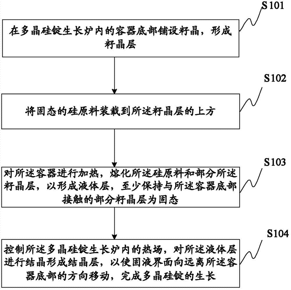
[0111] Based on the above research, an embodiment of the present invention provides a method for manufacturing a polycrystalline silicon ingot, the flow chart of the method is as follows figure 1 shown, including the following steps:

[0112] Step S101: laying seed crystals on the bottom of the container in the polycrystalline silicon ingot growth furnace to form a seed crystal layer;

[0113] Wherein, the seed crystal layer may be a whole large single crystal seed crystal which is substantially the same size and shape as the bottom of the container, or may be formed by splicing multiple small single crystal seed crystals. Moreover, the seed crystal is single crystal silicon with a fixed crystallographic orientation, and the seed layer includes at least one single crystal silicon layer with crystallographic orientation. Preferably, the seed crystals in this embodiment are (100), ( 110) or (111) oriented single crystal silicon.

[0114] Specifically, in this embodiment, the s...

Embodiment 2

[0136] In the normal ingot casting process, after the crystal growth is completed, the crystal needs to be cooled to a certain temperature, the polysilicon ingot is removed from the ingot furnace, and then the polysilicon ingot is further processed.

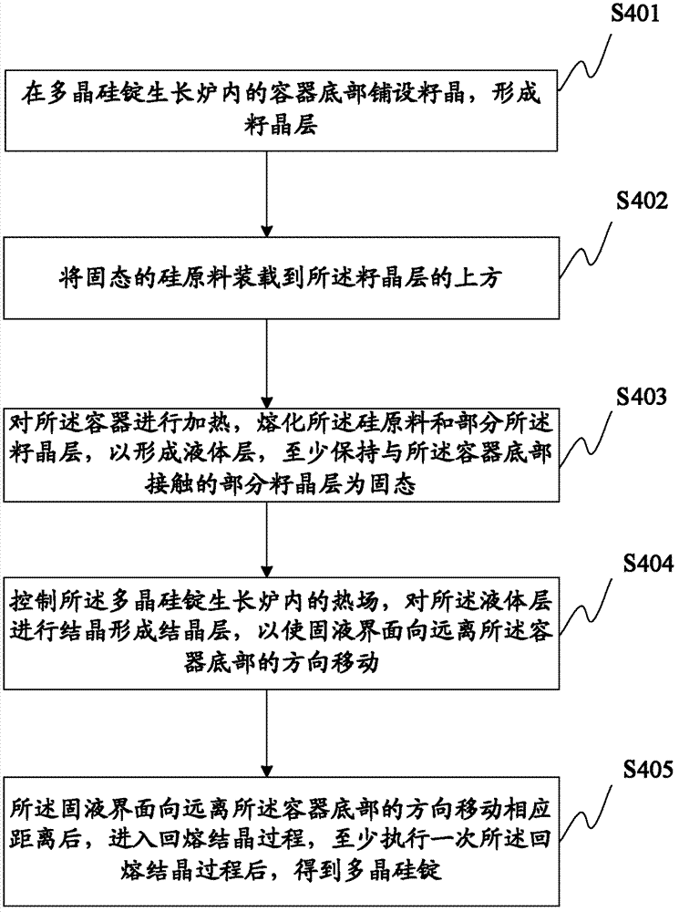
[0137] As described in step 104 in Example 1, the crystallization rate of molten silicon will affect the quality of the final product, and the hard spots and impurity-enriched layers in the product can be reduced by slowing down the growth rate, but due to the initial stage of crystallization , the growth rate of the crystal is more difficult to control, in order to avoid the above-mentioned defects, therefore, on the basis of the first embodiment, this embodiment figure 1 The process of completing the crystal growth in step S104 is further defined, and the specific process of forming the polycrystalline silicon ingot is described in detail.

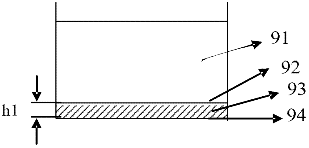
[0138] see figure 2 In this embodiment, control the thermal field in the polysilicon ...

Embodiment 3

[0148] The flow chart of the method for manufacturing polycrystalline silicon ingots disclosed in this embodiment is shown in Figure 4. The difference from the above two embodiments is that in this embodiment, the selection of the seed crystal, the formation method of the seed crystal layer, and the method of loading the silicon raw material process concrete, Figure 4 Only the method in embodiment two is used as an example for illustration. Of course, the method in this embodiment can also be applied to the method in embodiment one. The method in this embodiment includes the following steps:

[0149] Step S201: at the bottom of the container in the polycrystalline silicon ingot growth furnace, the seed crystal layer is formed by splicing and tiling seed crystals with the same crystallographic orientation, and the seed crystal layer is substantially parallel to the bottom of the container;

[0150] In this embodiment, it is preferable to use (100)-oriented monocrystalline sili...


PUM

PropertyMeasurementUnit
thicknessaaaaaaaaaa
thicknessaaaaaaaaaa
thicknessaaaaaaaaaa

Abstract

The invention discloses a manufacturing method of a polycrystalline silicon ingot. The manufacturing method comprises the steps of paving seed crystals on the bottom of a container in a polycrystalline silicon ingot growth furnace to form a seed crystal layer; loading solid silicon raw materials on the seed crystal layer; heating the container to melt the silicon raw materials and part of seed crystal layer to form a liquid layer, and at least keeping part of the seed crystal layer contacted with the bottom of the container to be in the solid state; controlling a thermal field in the polycrystalline silicon ingot growth furnace, and crystallizing the liquid layer to form a crystallization layer so as to move a solid-liquid interface to the direction far away from the bottom of the container to complete the growth of the polycrystalline silicon ingot. The polycrystalline silicon ingot produced by adopting the method disclosed by the invention is low in impurity content, the produced solar cell is low in cost and attenuation coefficient, and the photoelectric conversion efficiency is high.

Description

technical field [0001] The invention relates to the manufacturing technology of monocrystalline silicon and polycrystalline silicon and the field of optoelectronics, in particular to a polycrystalline silicon ingot, a manufacturing method thereof, and a solar battery. Background technique [0002] Solar cells can convert light energy into electrical energy. The photoelectric conversion efficiency and the speed of battery attenuation are important parameters to measure the quality of solar cells. At present, according to different materials, solar cells are mainly divided into two types: monocrystalline silicon solar cells and polycrystalline silicon solar cells. [0003] Among them, the monocrystalline silicon ingot is formed by melting the silicon raw material containing dopant, and then pulling the crystalline silicon out of the melting region to crystallize. Usually, the method of producing single crystal silicon ingot is the melt Czochralski method (Czochralski method, r...

Claims


Application Information

Patent Timeline
Patent Type & Authority Patents(China)
IPC IPC(8): C30B28/06C30B29/06H01L31/0368G01F23/04
CPCY02E10/50
Inventor 郑志东汤旋彭春球石郧熙翟蕊李娟刘文涛
Owner ZHEJIANG YUHUI SOLAR ENERGY SOURCE
Why Eureka
Try Eureka