Polycrystalline silicon ingot, manufacturing method thereof, solar cell

A technology of polycrystalline silicon ingots and manufacturing methods, which is applied in the direction of polycrystalline material growth, chemical instruments and methods, circuits, etc., can solve the problems of low photoelectric conversion efficiency, low minority carrier lifetime, and small crystal grains, and achieve high photoelectric conversion efficiency and reduce The effect of oxygen impurity content and low attenuation coefficient

Inactive Publication Date: 2016-02-10
ZHEJIANG YUHUI SOLAR ENERGY SOURCE
View PDF11 Cites 0 Cited by
  • Summary
  • Abstract
  • Description
  • Claims
  • Application Information

AI Technical Summary

Problems solved by technology

Compared with monocrystalline silicon ingots, there are more defects in polycrystalline silicon ingots, the grains are small, and there are more grain boundaries and dislocations between conventional polycrystalline silicon grains, resulting in rapid recombination of charge carriers, resulting in low minority carrier lifetime. , and, because the orientation between crystal grains is random, it is difficult to texture the surface of the wafer well, so that the photoelectric conversion efficiency of conventional polycrystalline silicon solar cells is lower than that of monocrystalline silicon solar cells, but the oxygen content in polycrystalline silicon ingots It can be controlled at a good level, so that the attenuation coefficient of polycrystalline silicon solar cells is low

Method used


Image

  • Polycrystalline silicon ingot, manufacturing method thereof, solar cell
  • Polycrystalline silicon ingot, manufacturing method thereof, solar cell
  • Polycrystalline silicon ingot, manufacturing method thereof, solar cell

Examples


Embodiment 1

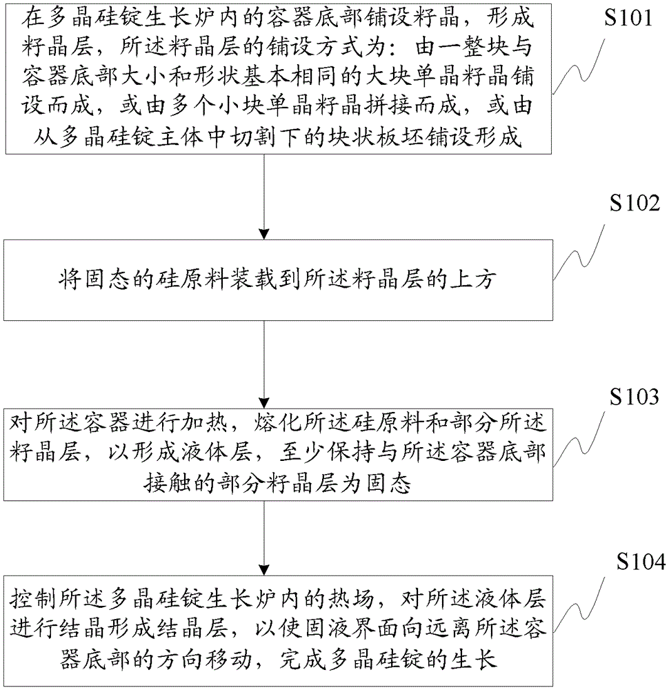
[0062] Based on the above research, an embodiment of the present invention provides a method for manufacturing a polycrystalline silicon ingot, the flow chart of the method is as follows figure 1 shown, including the following steps:

[0063] Step S101: laying seed crystals on the bottom of the container in the polycrystalline silicon ingot growth furnace to form a seed crystal layer, wherein the seed crystal layer is a bulk single crystal seed crystal that is substantially the same size and shape as the bottom of the container, or formed by Multiple small single crystal seed crystals spliced ​​together;

[0064] Wherein, the seed crystal is single crystal silicon with a fixed crystallographic orientation, and the seed layer includes at least one single crystal silicon layer with crystallographic orientation. Preferably, the seed crystals in this embodiment are (100), ( 110) or (111) oriented single crystal silicon.

[0065] Specifically, in this embodiment, the seed layer i...

Embodiment 2

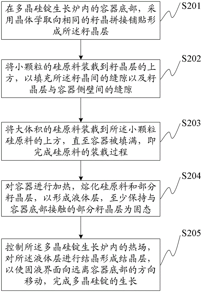
[0083] The flow chart of the casting method of the polycrystalline silicon ingot disclosed in this embodiment is as follows: figure 2 As shown, the difference from the previous embodiment is that in this embodiment, the selection of the seed crystal, the formation method of the seed layer and the process of loading silicon raw materials are embodied, and the method includes the following steps:

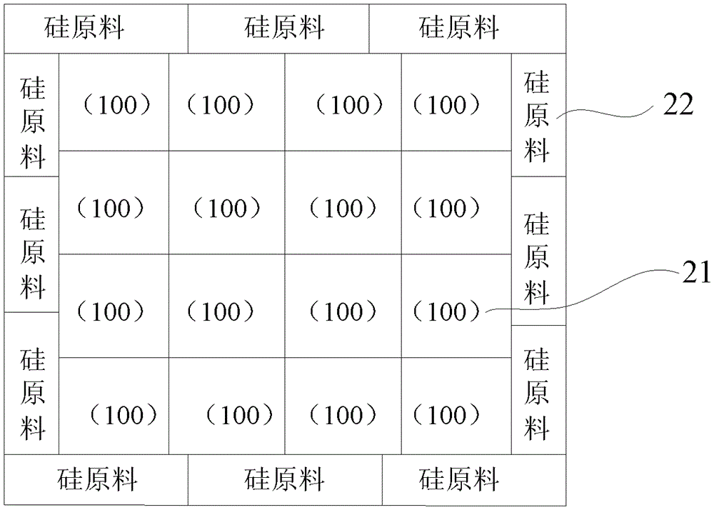
[0084] Step S201: at the bottom of the container in the polycrystalline silicon ingot growth furnace, the seed crystal layer is formed by splicing and tiling seed crystals with the same crystallographic orientation, and the seed crystal layer is substantially parallel to the bottom of the container;

[0085] In this embodiment, the seed layer is preferably formed by paving (100)-oriented single crystal silicon. Preferably, the area of ​​the seed layer accounts for the percentage of the bottom area of ​​the container, that is, the area of ​​the seed layer is The area accounts for 50%-...

Embodiment 3

[0093] The difference from the previous embodiment is that the laying method of the seed layer and the selection of the seed crystal in this embodiment are different, and the crystallographic orientation of the seed crystal in this embodiment is different. The flow chart of the casting method of the polycrystalline silicon ingot disclosed in this embodiment is as follows: Figure 5 As shown, the method includes the following steps:

[0094] Step S301: splicing and paving seed crystals with the first crystallographic orientation to cover part of the bottom area of ​​the container to form a seed crystal region with the first crystallographic orientation;

[0095] Step S302: using a seed crystal with a second crystallographic orientation to cover part of the bottom area of ​​the container to form a seed crystal region with a second crystallographic orientation, the seed crystal region with a first crystallographic orientation and the seed crystal region with a first crystallograp...


PUM

PropertyMeasurementUnit
thicknessaaaaaaaaaa
thicknessaaaaaaaaaa
thicknessaaaaaaaaaa

Abstract

The invention discloses a preparation method for a polycrystalline silicon ingot. The preparation method comprises the following steps of: paving seed crystals on the bottom of a container in a polycrystalline silicon ingot growth furnace to form a seed crystal layer, wherein the seed crystal layer can be formed by paving a whole large single-crystal seed crystal of which the size and the shape are the same as those of the bottom of the container, or splicing a plurality of small single-crystal seed crystals, or paving blocky plate blanks cut from polycrystalline silicon main bodies; loading solid silicon raw materials above the seed crystal layer; heating the container, smelting the silicon raw materials and part of the seed crystal layer to form a liquid layer, and at least keeping part of the seed crystal layer contacted with the bottom of the container in a solid state; and controlling a thermal field in the polycrystalline silicon ingot growth furnace, and crystallizing the liquid layer to form a crystallizing layer to ensure that a solid interface moves toward the direction far away from the bottom of the container so as to finish growing the polycrystalline silicon ingot. The polycrystalline silicon ingot produced by the method is low in impurity content, and the produced solar cell is low in cost and attenuation coefficient and high in photoelectric conversion efficiency.

Description

technical field [0001] The invention relates to the manufacturing technology of monocrystalline silicon and polycrystalline silicon and the field of optoelectronics, in particular to a polycrystalline silicon ingot, a manufacturing method thereof, and a solar battery. Background technique [0002] Solar cells can convert light energy into electrical energy. The photoelectric conversion efficiency and the speed of battery attenuation are important parameters to measure the quality of solar cells. At present, according to different materials, solar cells are mainly divided into two types: monocrystalline silicon solar cells and polycrystalline silicon solar cells. [0003] Among them, the monocrystalline silicon ingot is formed by melting the silicon raw material containing dopant, and then pulling the crystalline silicon out of the melting region to crystallize. Usually, the method of producing single crystal silicon ingot is the melt Czochralski method (Czochralski method, r...

Claims


Application Information

Patent Timeline
Patent Type & Authority Patents(China)
IPC IPC(8): C30B28/06C30B29/06H01L31/028
CPCY02E10/547
Inventor 郑志东翟蕊石郧熙李娟刘文涛彭春球
Owner ZHEJIANG YUHUI SOLAR ENERGY SOURCE
Why Eureka
Try Eureka