Confinement layer structure and its manufacturing method, semiconductor laser and its manufacturing method

A manufacturing method and laser technology, applied to the structure of semiconductor lasers, lasers, and optical waveguide semiconductors, can solve problems such as high Al content and performance degradation of semiconductor lasers, and achieve improved performance, improved conductivity, and improved slope efficiency Effect

Active Publication Date: 2021-04-20
SUZHOU EVERBRIGHT PHOTONICS CO LTD +1
View PDF9 Cites 0 Cited by
  • Summary
  • Abstract
  • Description
  • Claims
  • Application Information

AI Technical Summary

Problems solved by technology

[0004] Therefore, the technical problem to be solved in the present invention is to overcome the defect that the high content of Al component in the confinement layer of the traditional semiconductor laser in the prior art causes the performance degradation of the semiconductor laser

Method used


Image

  • Confinement layer structure and its manufacturing method, semiconductor laser and its manufacturing method
  • Confinement layer structure and its manufacturing method, semiconductor laser and its manufacturing method
  • Confinement layer structure and its manufacturing method, semiconductor laser and its manufacturing method

Examples


Embodiment 1

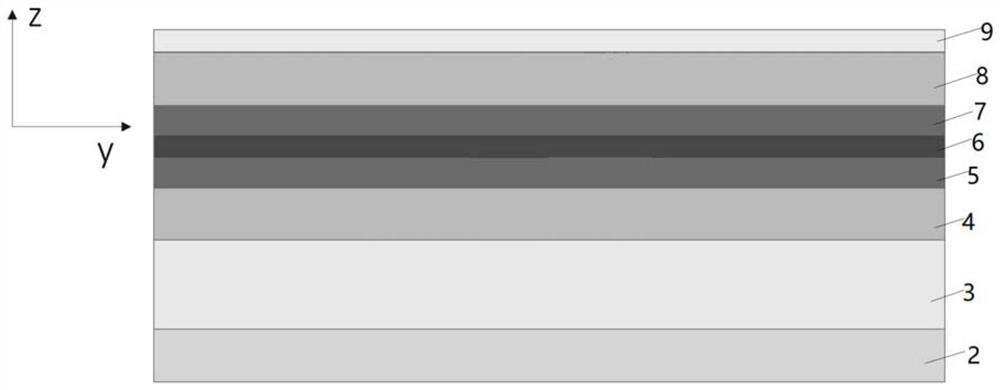
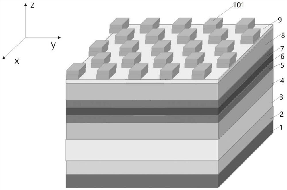
[0041] This embodiment provides a semiconductor laser, see Figure 1 to Figure 5 , which includes an N-type GaAs (gallium arsenide) substrate, a semiconductor laser structure, a P-type GaAs cap layer 9 and a confinement layer structure 10 arranged in sequence from bottom to top. Wherein, the confinement layer structure may also be referred to as a mixed confinement layer.

[0042]Wherein, the semiconductor laser structure described in the embodiment of the present invention mainly refers to other functional layer structures in the semiconductor laser except the substrate, the upper confinement layer, and the contact layer. The semiconductor laser structure is located above the N-type GaAs substrate 1, which includes N Type GaAs buffer layer 2, N-type AlGaAs (aluminum gallium arsenide) lower confinement layer, N-type AlGaAs lower waveguide layer 4, GaAs quantum barrier layer 5, InGaAs (gallium indium arsenide) quantum well layer, GaAs quantum barrier layer 7 and P-type AlGaAs ...

Embodiment 2

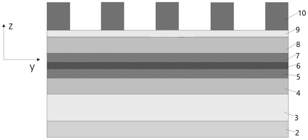
[0053] This embodiment provides a method for manufacturing a semiconductor laser, such as Figure 6 and Figure 7 As shown, it includes the following steps:

[0054] S11: growing a semiconductor laser structure on a substrate. Specifically, the substrate is an N-type GaAs substrate 1, which is first grown into an N-type GaAs substrate 1 in a Metal-organic Chemical Vapor Deposition (MOCVD) device, and then sequentially grown on an N-type GaAs substrate. 1 grow N-type GaAs buffer layer 2, N-type AlGaAs lower confinement layer 3, N-type AlGaAs lower waveguide layer 4, GaAs quantum barrier layer 5, InGaAs quantum well layer 6, GaAs quantum barrier layer 7 and P-type AlGaAs upper waveguide layer 8. Alternatively, the substrate and the semiconductor laser structure can be grown in a molecular beam epitaxy (MBE) device.

[0055] S12: growing a capping layer on the semiconductor laser. Specifically, the capping layer is a P-type GaAs capping layer with a thickness of 5nm-10nm. Th...


PUM

PropertyMeasurementUnit
thicknessaaaaaaaaaa

Abstract

The present invention provides a confinement layer structure and its fabrication method, a semiconductor laser and its fabrication method. The confinement layer structure includes several dielectric mask blocks distributed at intervals and confinement layers formed in gaps between the several dielectric mask blocks, wherein In the confinement layer, the gallium arsenide layer is used to replace the existing aluminum gallium arsenide layer, thereby forming a confinement layer mixed with a dielectric mask block and a gallium arsenide confinement layer. Since the refractive index of gallium arsenide is greater than that of aluminum gallium arsenide, and the refractive index of the dielectric mask block is smaller than that of aluminum gallium arsenide, the refractive index of the formed mixed confinement layer can be compared with that of the existing aluminum gallium arsenide (Al composition 40‑ 90%), which can guarantee its optical confinement effect. The conductivity of the resulting mixed confinement layer is better than that of aluminum gallium arsenide (Al composition 40-90%). The conductivity of the hybrid confinement layer is improved and the content of oxygen impurities is reduced, which will eventually reduce the threshold current of the semiconductor laser, increase its slope efficiency and COMD threshold, and improve the performance of the semiconductor laser.

Description

technical field [0001] The invention relates to the technical field of semiconductor lasers, in particular to a confinement layer structure and a manufacturing method thereof, a semiconductor laser and a manufacturing method thereof. Background technique [0002] Semiconductor lasers have many advantages such as small size, high efficiency, long life, and easy integration. High beam quality and narrow linewidth semiconductor lasers have higher beam quality, smaller slow axis divergence angle and narrower spectral linewidth, and are more suitable for large-scale semiconductor laser beam shaping and combining. It has a wide range of applications in industry, military, medical, national defense and other fields. [0003] The structure of a semiconductor laser generally includes a substrate, a lower confinement layer, a lower waveguide layer, an active region, an upper waveguide layer, an upper confinement layer, and a contact layer. In the traditional 8XX and 9XX semiconducto...

Claims


Application Information

Patent Timeline
Patent Type & Authority Patents(China)
IPC IPC(8): H01S5/20H01S5/22
CPCH01S5/2018H01S5/2206
Inventor 程洋王俊谭少阳廖新胜潘华东李泉灵
Owner SUZHOU EVERBRIGHT PHOTONICS CO LTD
Why Eureka
Try Eureka