A direct light-emitting micro-display array device and its preparation method

A light-emitting, micro-display technology, applied in the direction of electric solid-state devices, semiconductor devices, electrical components, etc., can solve the problems that have not yet been applied in the field of industrial production, poor insulation performance of buffer layer, and easy fracture of climbing metal, so as to improve stability And the reliability of the device, the reduction of steps, and the effect of reducing electrode crowding

Inactive Publication Date: 2015-10-28
BEIJING UNIV OF TECH
View PDF4 Cites 0 Cited by
  • Summary
  • Abstract
  • Description
  • Claims
  • Application Information

AI Technical Summary

Problems solved by technology

Invention patent 200720093946.2 presents the manufacturing method of AlGaInP-LED micro-display devices. The upper and lower isolation grooves are etched by ICP technology to realize the separation of the LED light-emitting layer and the light-transmitting layer. However, there are many shortcomings that prevent it from being applied to the actual industrial production field.
At present, the isolation of devices is mainly realized by dry etching. However, the mesa structure by dry etching will bring some problems: if the step is too deep, the climbing metal will be easily broken; if the insulation performance of the buffer layer is poor, it will cause leakage.
At the same time, physical effects such as spontaneous polarization and piezoelectric polarization unique to III-V materials are very sensitive to device interface characteristics, thus limiting the application of conventional ICP and other processes in the preparation of high-density display arrays

Method used


Image

  • A direct light-emitting micro-display array device and its preparation method
  • A direct light-emitting micro-display array device and its preparation method
  • A direct light-emitting micro-display array device and its preparation method

Examples


Embodiment Construction

[0033] The direct light-emitting display array of the present invention will be described in detail below in conjunction with the accompanying drawings:

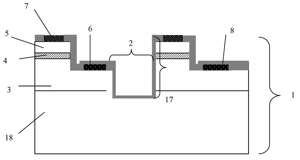
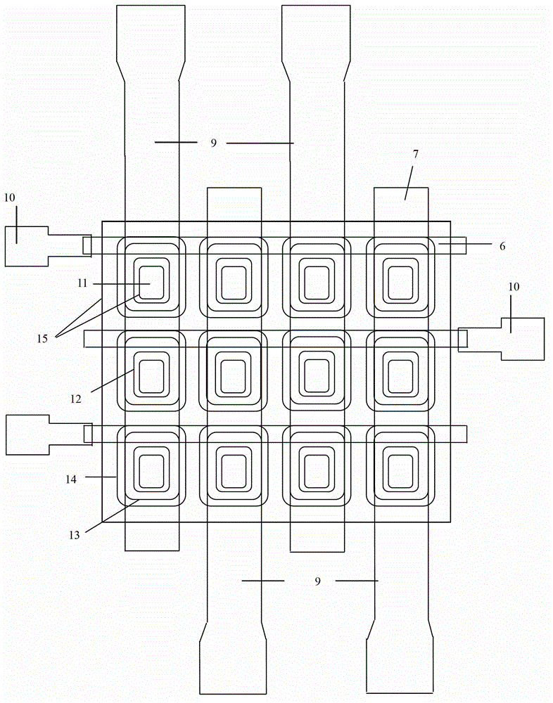
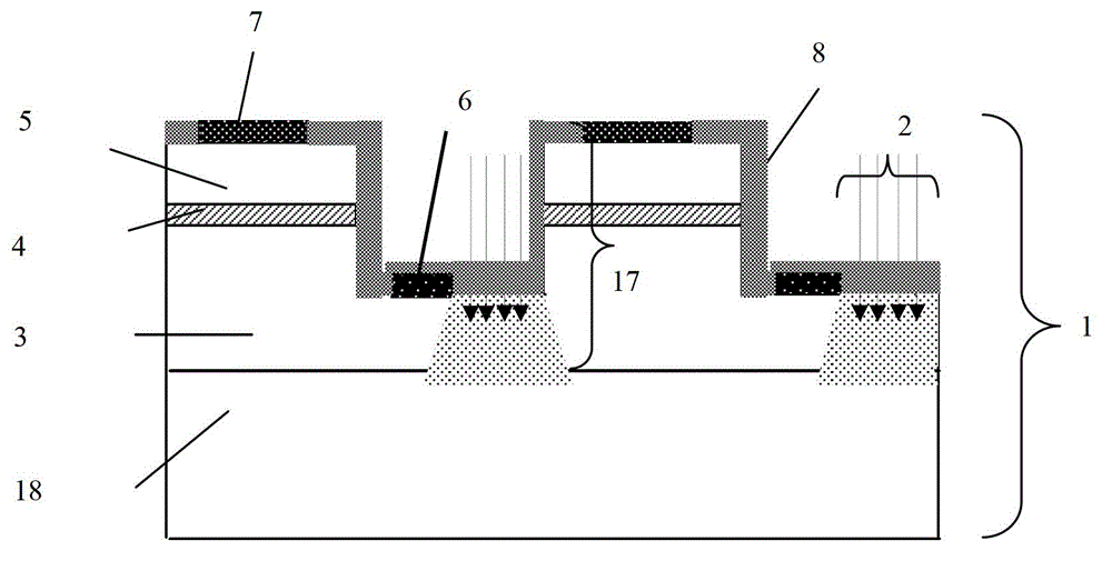
[0034] Such as Figures 3 to 5 As shown, a direct light-emitting microdisplay array of the present invention is characterized in that it includes an epitaxial wafer 1, a semiconductor matrix unit 17, a semiconductor matrix isolation region 2, an n-type conductive layer 3, a light-emitting layer 4, a p-type conductive layer 5, n Electrode 6, p-electrode 7, isolation protection layer 8, anode line 9, cathode line 10; dry etching method is adopted on the epitaxial wafer 1, and the etching part reaches the n-type conductive layer 3 to form a plurality of semiconductor matrix units 17, Ions are implanted on the n-type conductive layer 3 exposed by etching until the substrate is formed to form a high-resistance region, and a semiconductor matrix isolation region 2 is obtained. n-electrodes 6 are arranged on the n-type conductive l...


PUM


Abstract

The invention relates to a direct-light-emitting-type micro display array device and a preparation method thereof. A display array comprises a substrate epitaxial wafer, semiconductor matrix isolating regions, electron-type conducting layers, light emitting layers, hole-type conducting layers, electron-type conducting electrodes, hole-type conducting electrodes, isolating protection layers, anode lines and cathode lines. The preparation method comprises the steps of: etching an epitaxial layer by adopting a dry-process etching method to obtain the electron-type conducting layers and form a plurality of array units; implanting ions into the electron-type conducting layers till to a substrate by adopting an ion implantation method to realize isolation of adjacent units and obtain the semiconductor matrix isolating regions; evaporating metal through electron beams to form the electron-type conducting electrodes and leading out the cathode lines; depositing the isolating protection layers through PECVD (Plasma Enhanced Chemical Vapor Deposition); and evaporating metal through electron beams to form the hole-type conducting electrodes and leading out the cathode lines, wherein regions formed by the anode lines and the cathode lines which are spatially intersected are display pixels.

Description

technical field [0001] The invention belongs to the field of semiconductor lighting, and in particular relates to a direct light-emitting micro-display array device and a preparation method thereof. technical background [0002] With the continuous improvement of people's material and cultural living standards, people's requirements for display technology are also getting higher and higher. Light-emitting diodes (LEDs) have the advantages of being all solid and high luminous efficiency, and they have all begun to be used in the fields of display and lighting. The semiconductor materials used for solid-state lighting are mainly III-V compounds. Among them, high-brightness solid-state lighting devices based on GaN-based and AlGaInP-based materials also have the advantages of small size, long life, and low power. LEDs have been widely used in full-color display imaging devices, and the development of display technology has also risen accordingly. Invention patent 200720093946...

Claims


Application Information

Patent Timeline
Patent Type & Authority Patents(China)
IPC IPC(8): H01L27/15H01L33/62H01L33/00
Inventor 郭伟玲丁艳朱彦旭刘建朋
Owner BEIJING UNIV OF TECH
Why Eureka
Try Eureka