LED packaged structure and surface roughening method for same

A technology of LED packaging and LED packaging body, which is applied in the direction of semiconductor devices, electrical components, circuits, etc., can solve problems such as process difficulties, silica gel adhesion, and difficulty in production, and achieve the effect of improving luminous efficiency

Active Publication Date: 2015-02-18
北京易美新创科技有限公司
View PDF6 Cites 0 Cited by
  • Summary
  • Abstract
  • Description
  • Claims
  • Application Information

AI Technical Summary

Problems solved by technology

However, it is difficult to roughen the LED package made of packaging materials such as silica gel or epoxy glue. If the surface of the LED package is roughened by compression molding, there will be a phenomenon of silica gel adhesion.
It is even more difficult to realize its production

Method used


Image

  • LED packaged structure and surface roughening method for same
  • LED packaged structure and surface roughening method for same
  • LED packaged structure and surface roughening method for same

Examples


Embodiment 2

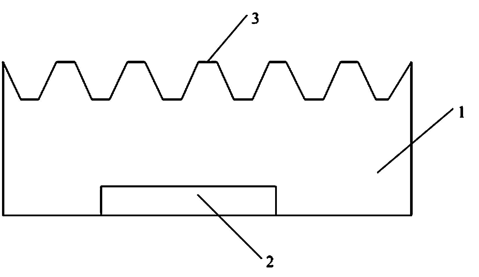
[0030] Such as figure 2 As shown, Embodiment 2: The difference between this embodiment and Embodiment 1 is that the cross-section of the concave-convex structure 3 is trapezoidal.

Embodiment 3

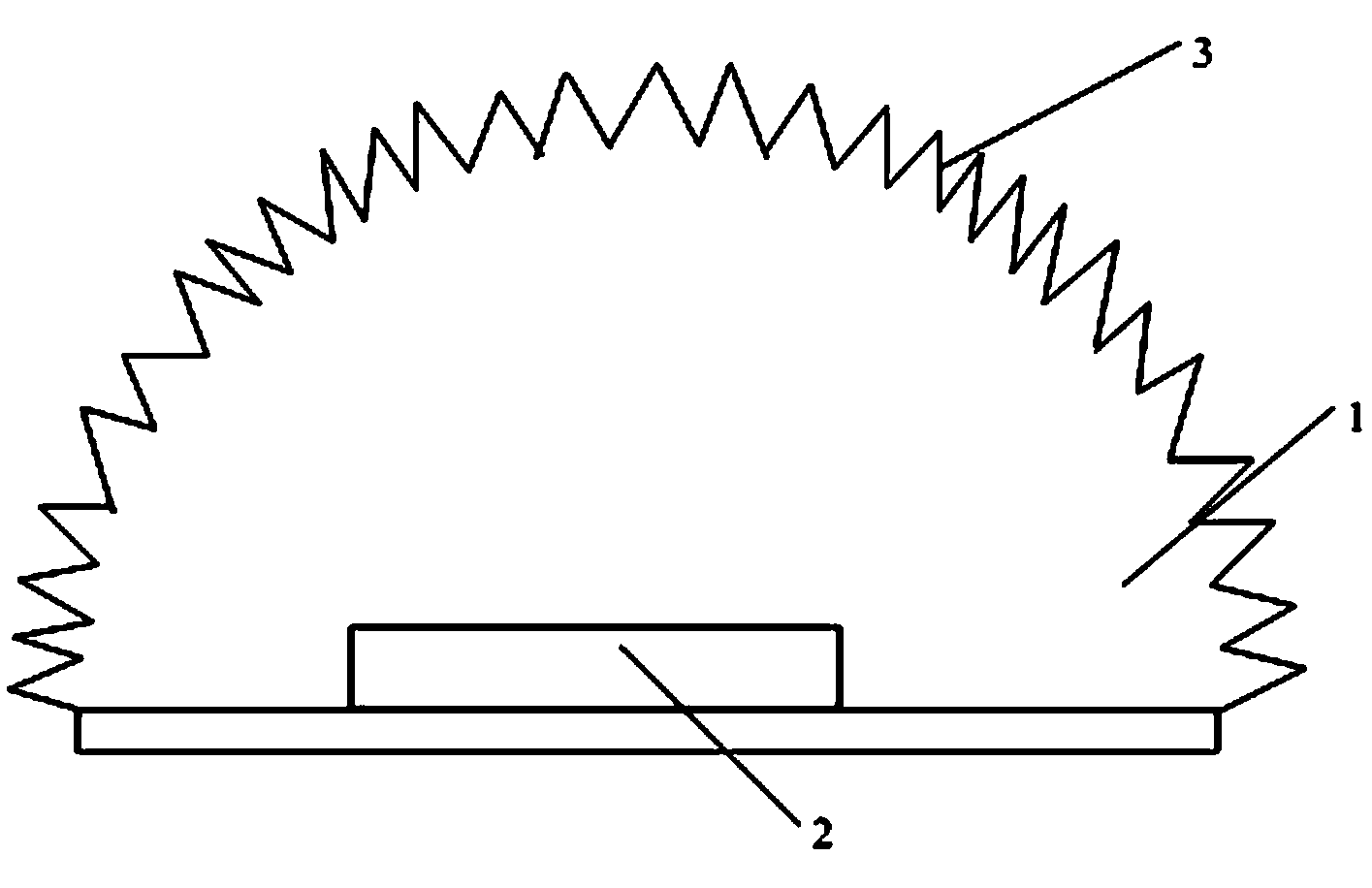
[0031] Such as image 3 , as shown, Embodiment 3: The difference between this embodiment and Embodiment 1 is that the surface of the LED package is protruding, and its cross-section is arc-shaped. The surface of such an LED package is roughened, and the requirements for the plastic film It has strong flexibility.

[0032] Such as Figure 4 As shown, a method for roughening the surface of an LED packaging structure, it comprises the following steps:

[0033] Step 1: Make a concave-convex structure on the plastic film. If the concave-convex structure on the plastic film is a regular geometric shape, it can be made with a photolithography mold, or compression molded with a compression mold. The concave-convex structure is a microstructure (must be optically A crystal structure that can only be observed with a microscope or an electron microscope), according to the size of the plastic film, and the depth and shape of the predetermined concave-convex structure, the distribution o...


PUM


Abstract

The invention relates to an LED packaged structure which comprises an LED packaged body and an LED chip arranged in the LED packaged body. A periodic concave-convex structure is arranged on the surface of the LED packaged body. The invention further relates to a surface roughening method for the LED packaged structure. The LED packaged structure and the surface roughening method have the advantages that the concave-convex structure is formed on the LED packaged structure, so that surfaces of the LED packaged body are roughened simply and effectively, and the luminous efficiency of an efficient LED is enhanced.

Description

technical field [0001] The invention relates to an LED packaging structure and a method for realizing its surface roughening. Background technique [0002] The improvement of the luminous efficiency of high-power LED can not only be improved through the improvement of quantum efficiency in the LED chip, but also can be improved by increasing the extraction efficiency of LED photons. The surface roughening of the chip is an effective method to improve the extraction efficiency of LED photons. According to Snell's law, when light is incident from a medium with a higher refractive index to a medium with a lower refractive index, the light with an incident angle greater than the critical angle will be reflected back to the original medium. For LED grains, the refractive index of the grain material is often higher than that of the outer packaging material, such as silica gel or epoxy resin, so the light emitted by the light-emitting layer in the grains only has a chance of light...

Claims


Application Information

Patent Timeline
Patent Type & Authority Patents(China)
IPC IPC(8): H01L33/48H01L33/54H01L33/00
Inventor 刘国旭
Owner 北京易美新创科技有限公司
Why Eureka
Try Eureka