Methods of purifying silicon

A technology of elemental silicon and crucible, which is applied in chemical instruments and methods, single crystal growth, polycrystalline material growth and other directions, can solve the problems of instability of growth interface, and achieve the effects of reducing enrichment, accelerating transmission and improving interface stability.

Active Publication Date: 2020-06-05
湖南鸿新实业有限责任公司
View PDF6 Cites 0 Cited by
  • Summary
  • Abstract
  • Description
  • Claims
  • Application Information

AI Technical Summary

Problems solved by technology

[0003] Traditionally, directional solidification is mainly used to purify polysilicon by metallurgy. However, due to the addition of metallurgical elements, the solidification temperature interval of primary silicon is greatly increased. Ordinary directional solidification devices can easily destabilize the growth interface and introduce a large number of metal inclusions. Therefore, the corresponding inclusions must be removed by polysilicon crusher pickling and other processes in the follow-up

Method used


Image

  • Methods of purifying silicon
  • Methods of purifying silicon
  • Methods of purifying silicon

Examples


Embodiment Construction

[0026] The technical solutions in the embodiments of the present invention are clearly and completely described below in conjunction with the accompanying drawings in the embodiments of the present invention. Obviously, the described embodiments are only part of the embodiments of the present invention, not all of them. Based on the embodiments of the present invention, all other embodiments obtained by persons of ordinary skill in the art without making creative efforts belong to the protection scope of the present invention.

[0027] In the following description, a lot of specific details are set forth in order to fully understand the present invention, but the present invention can also be implemented in other ways different from those described here, and those skilled in the art can do it without departing from the meaning of the present invention. By analogy, the present invention is therefore not limited to the specific examples disclosed below.

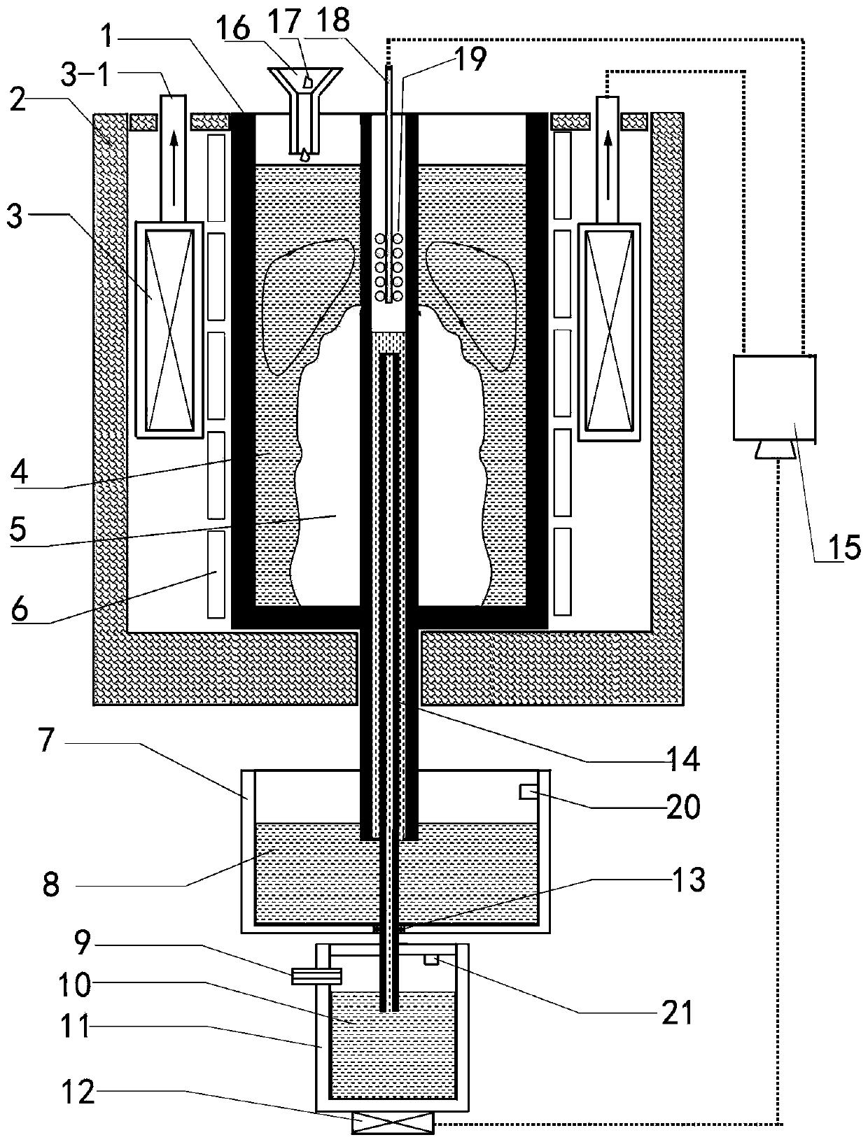
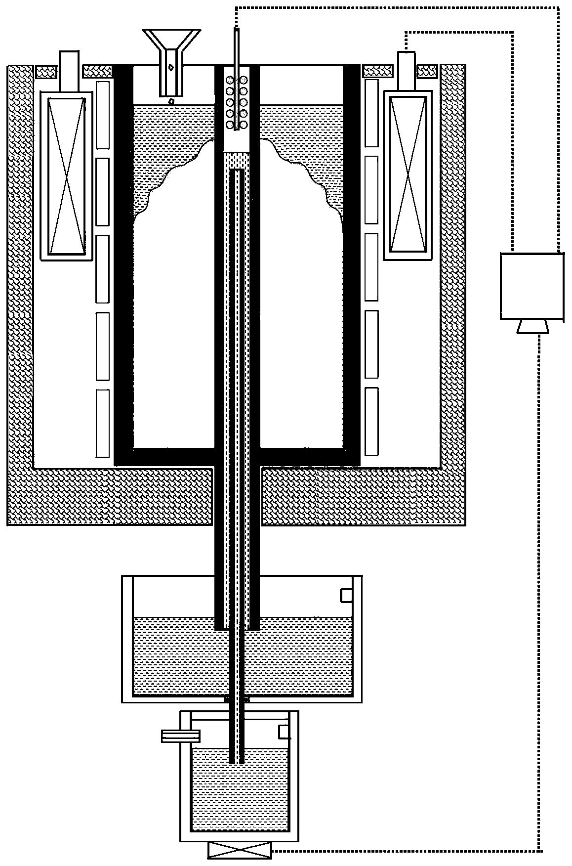
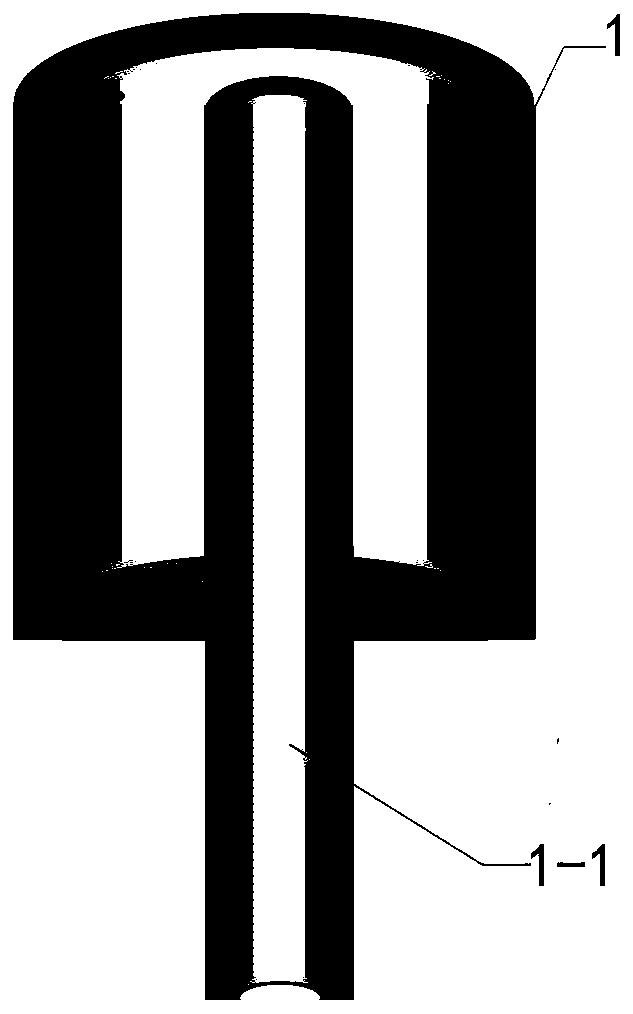
[0028] Such as figure...


PUM


Abstract

The invention discloses a method for purifying silicon. The method comprises the steps: firstly, melting crude silicon and high-purity metal capable of forming hypereutectic or hyperperitectic with silicon in a crucible in which a temperature directional control tube is arranged; high lateral and longitudinal temperature gradients are generated by utilizing a temperature directional control tube,and the crystallization process of the primary monatomic silicon in a hypereutectic alloy system is controlled by combining a traveling wave magnetic field, so that the stability of a growth interfaceof the primary monatomic silicon is improved, and the formation of fluxing metal inclusions is inhibited. Firstly, the prepared bar is of a structure that the primary monatomic silicon is located inthe center and the fluxing metal is located on the outer side. Then, supersaturated dissolution of silicon is realized in a top high-temperature region, and coarsening growth of the central primary monatomic silicon rod is realized by virtue of reciprocating motion of a traveling wave magnetic field generator; and after the growth is finished and cooling is performed, the head metal gettering areais cut off. The process is repeated again on the obtained primary silicon to prepare the high-purity silicon. Therefore, according to the method, introduction of a large number of metal inclusions can be avoided, the process is simple, and the prepared silicon is high in purity.

Description

technical field [0001] The invention relates to the technical field of semiconductor silicon, in particular to a method for purifying silicon. Background technique [0002] With the depletion of petroleum energy, solar energy as an inexhaustible clean energy has attracted the attention of countries all over the world, and solar-grade silicon materials are the basis for preparing solar cells. The metallurgical method is a method of preparing solar-grade polysilicon, which is economical, simple in process and less polluting to the environment. Therefore, it has become the best method for preparing solar-grade silicon materials. It can quickly remove metal impurities from silicon, and then pass through regional smelting , Electron beam high-temperature vacuum smelting can effectively remove elements with high saturated vapor pressure, such as phosphorus. [0003] Traditionally, directional solidification is mainly used to purify polysilicon by metallurgy. However, due to the a...

Claims


Application Information

Patent Timeline
Patent Type & Authority Patents(China)
IPC IPC(8): C30B29/06C30B9/10
CPCC30B9/10C30B29/06
Inventor 李超
Owner 湖南鸿新实业有限责任公司
Why Eureka
Try Eureka