Method for measuring carrier concentration in semiconductor quantum well

A technology of carrier concentration and measurement method is applied in the field of detection of characteristic parameters of semiconductor optoelectronic functional materials, which can solve the problems of narrow sub-band energy gap, difficulty in feasibility and measurement accuracy, and inability to resolve quantum well scale.

Active Publication Date: 2012-12-19
SHANGHAI INST OF TECHNICAL PHYSICS - CHINESE ACAD OF SCI
View PDF3 Cites 4 Cited by
  • Summary
  • Abstract
  • Description
  • Claims
  • Application Information

AI Technical Summary

Problems solved by technology

Corresponding to this is the development of profile measurement technology based on scanning probe microscopy in recent years. This type of method extracts the carrier concentration by detecting the electronic distribution of the cross-section of functional materials, but the specific scheme or spatial resolution cannot be resolved. Quantum well scale, such as scanning capacitance microscopy (SCM); or the interpretation of measured electronic information depends on artificially adjustable parameters, which cannot achieve unidirectional extraction of carrier concent

Method used


Image

  • Method for measuring carrier concentration in semiconductor quantum well
  • Method for measuring carrier concentration in semiconductor quantum well
  • Method for measuring carrier concentration in semiconductor quantum well

Examples


Embodiment Construction

[0042] The acquisition of the carrier concentration in a group of n-type doped GaAs / AlGaAs quantum wells will be described in detail below in conjunction with the accompanying drawings to the specific implementation of the present invention, but it is by no means limiting the present invention, that is, the present invention is by no means limited to this Example.

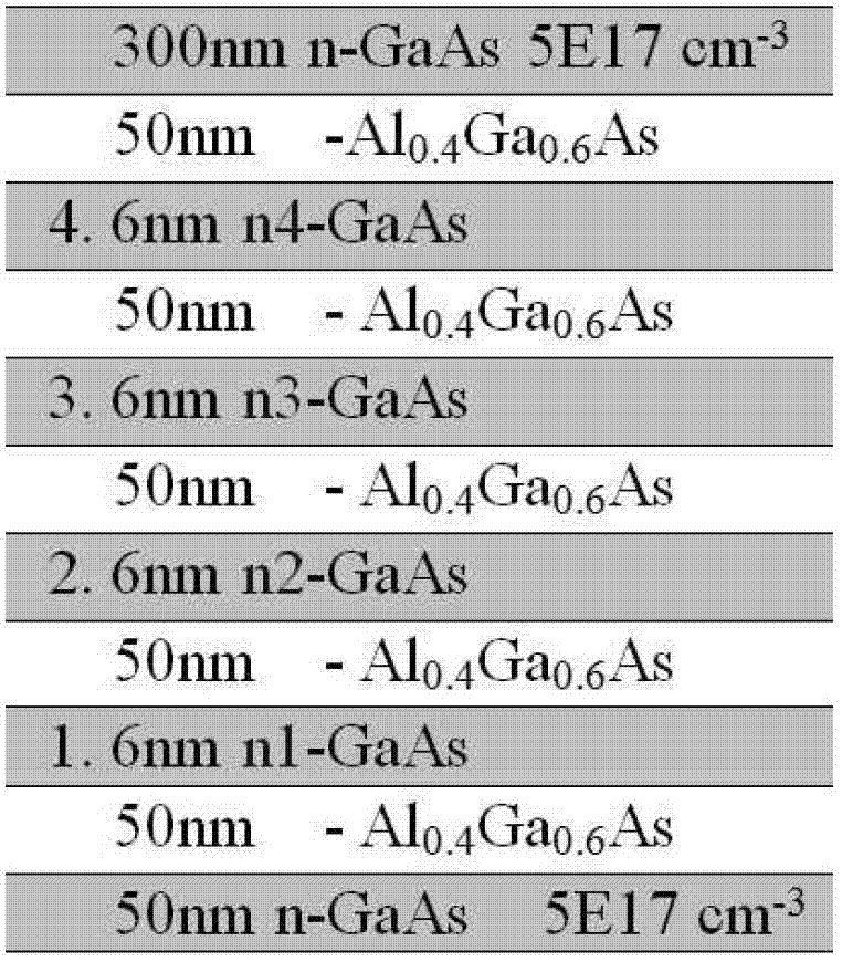
[0043] figure 1 A group of GaAs / AlGaAs doped quantum wells grown on GaAs (001) substrates used in the present invention, wherein the n-type doping concentration of each quantum well changes continuously within a certain range, and the width of the quantum wells is all 6nm; The sample also contains a known doping concentration of 5×10 17 cm -3 The n-type GaAs electrode layer is used for the electrical measurement calibration of the Schottky barrier height. Basic physical constants of GaAs quantum well materials: the effective mass of conduction band electrons is 0.063m 0 (m 0 is the rest mass of the electron), ...


PUM


Abstract

The invention discloses a method for measuring carrier concentration in a semiconductor quantum well. The method includes steps of measuring local conductance distribution of the cross section of the semiconductor quantum well by the electric detection mode of a scanning probe microscope; setting up a numerical model capable of reflecting relation between a conducting probe-quantum well Schottky contact conductivity and carrier concentration in the quantum well; and determining parameters and carrier concentration of the quantum well of the numerical model according to the measured conductivity distribution. The method is high in spatial discrimination and has advantages in analysis of a narrow quantum well and in coupling of the quantum well, is applicable to wider carrier concentration range from non-degeneracy to degeneracy doping conditions, and has significance value for analysis of internal performances of a semiconductor photoelectric device taking a quantum well as a functional structure.

Description

technical field [0001] The invention relates to the detection of characteristic parameters of semiconductor optoelectronic functional materials, in particular to a method for obtaining carrier concentration in semiconductor quantum wells. Background technique [0002] Migrating electrons or holes, i.e. charge carriers, in semiconductors are the functional carriers of modern (opto)electronic devices. In optoelectronic devices, the transition of carriers between different energy states corresponds to the absorption and emission of photons, thereby realizing the conversion between light energy and electrical energy. In view of this, the carrier concentration and its microscopic distribution characteristics in the semiconductor functional structure are the basic information to determine the performance of the device, especially in the semiconductor quantum functional structure. Whether it is a quantum well photodetector or a quantum cascade laser, its core Structure - The carri...

Claims


Application Information

Patent Timeline
IPC IPC(8): G01R19/00G01Q60/00
Inventor 李天信黄文超陆卫夏辉姚碧霂李宁李志锋
Owner SHANGHAI INST OF TECHNICAL PHYSICS - CHINESE ACAD OF SCI
Why Eureka
Try Eureka