[0021] The specific implementations of the touch liquid crystal grating and the 3D touch display device provided by the embodiments of the present invention will be described in detail below with reference to the accompanying drawings.
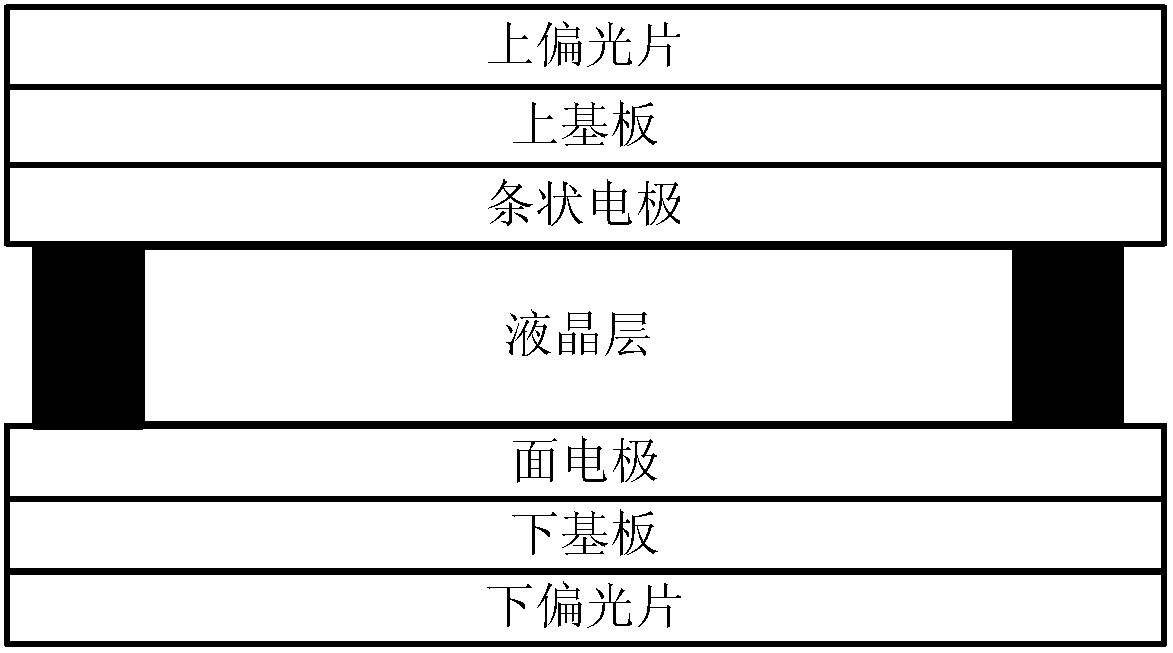
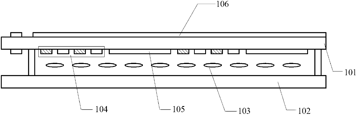
[0022] An embodiment of the present invention provides a touch liquid crystal grating, such as figure 2 As shown, it specifically includes: a first substrate 101, a second substrate 102, and a liquid crystal layer 103 filled between the first substrate 101 and the second substrate 102, and further includes:
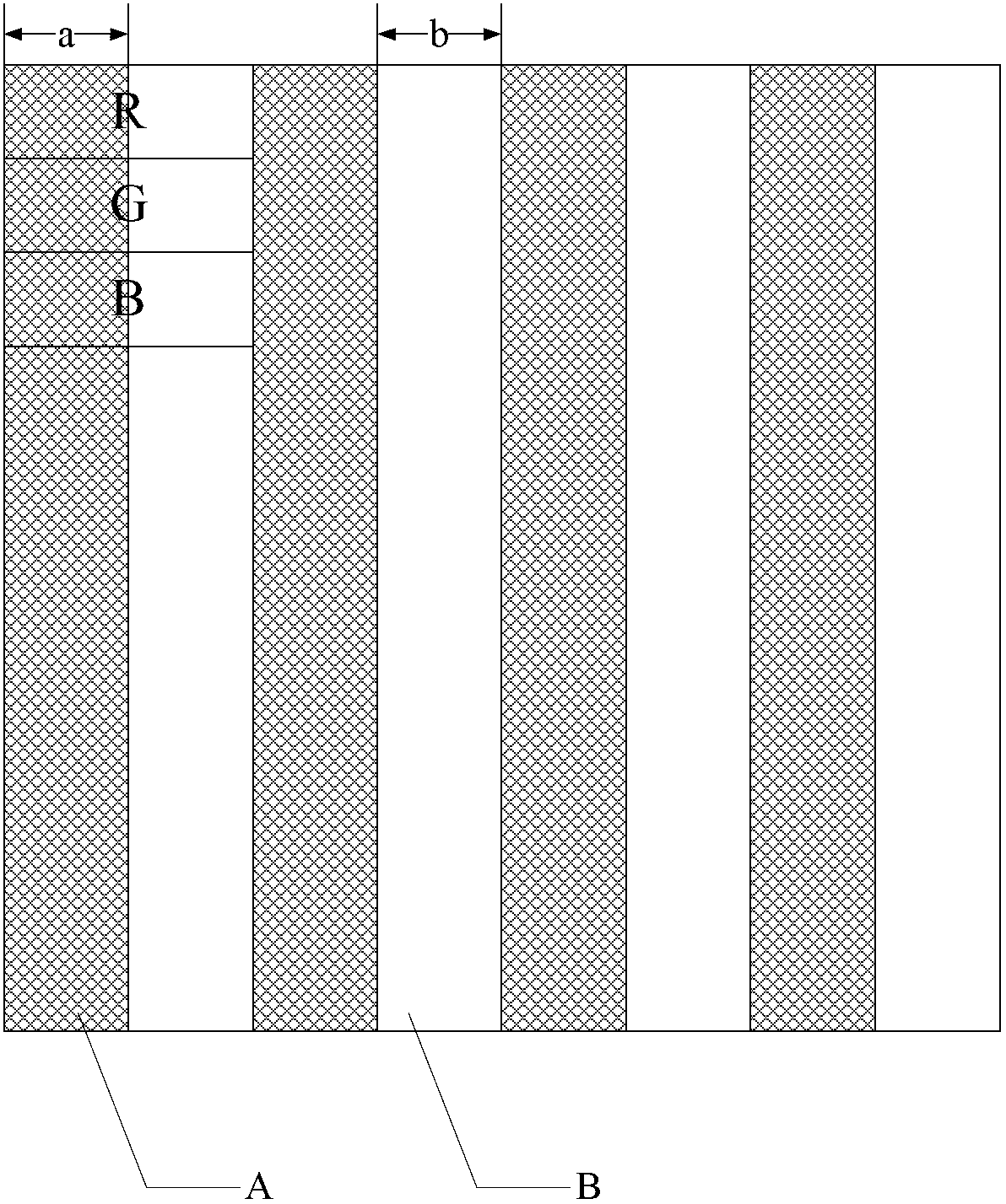
[0023] The grating electrodes 104 located on the side of the first substrate 101 facing the liquid crystal layer 103, each grating electrode 104 is located in the strip-shaped area A set at intervals; when the grating electrode 104 is energized, the liquid crystal molecules corresponding to the strip-shaped area A are generated Rotate, the liquid crystal molecules are aligned horizontally when not powered;
[0024] The touch drive electrodes 105 located on the side of the first substrate 101 facing the liquid crystal layer 103, and each touch drive electrode 105 is located in the interval area B between adjacent strip-shaped areas;
[0025] The touch sensing electrodes 106 located on the side of the first substrate 101 opposite to the liquid crystal layer 103 have different wiring directions from the touch sensing electrodes 106 and the touch driving electrodes 105.
[0026] Among them, in specific implementation, ITO (Indium Tin Oxides, indium tin metal oxide) material can be used as the grating electrode 104, the touch driving electrode 105, and the touch sensing electrode 106.
[0027] Preferably, the touch-sensitive liquid crystal grating is such as figure 2 As shown, it further includes: a first filter 107 on the side of the touch sensing electrode 106 that faces away from the liquid crystal layer 103, and a second filter 108 on the side of the second substrate 102 that faces away from the liquid crystal layer 103;
[0028] The light transmission axis directions of the first polarizer 107 and the second polarizer 108 are perpendicular or parallel to each other;
[0029] When power is not applied, the liquid crystal molecules in the liquid crystal layer 103 are aligned in parallel along the light transmission axis direction of the first polarizer or the second polarizer.
[0030] Specifically, when the light transmission axis directions of the first polarizer 107 and the second polarizer 108 are set to be parallel to each other, the liquid crystal molecules are aligned in parallel along the light transmission axis direction. At this time, the grating electrode 104 of the liquid crystal grating is not When power is applied, the liquid crystal molecules have no retardation effect on the polarized light passing through the second polarizer 108, and the polarized light passing through the liquid crystal molecules is consistent with the direction of the light transmission axis of the first polarizer 107. Therefore, in both the strip area A and the interval area B When the grating electrode 104 of the liquid crystal grating is energized, the liquid crystal molecules corresponding to the stripe area A rotate horizontally, which retards the polarized light passing through the second polarizer 108. The polarized light and the first polarized light The direction of the light transmission axis of the sheet 107 is different, the stripe-shaped area A forms a dark field, and the interval area B forms a bright field, forming a fringe grating. The above-mentioned structure can realize free conversion between 2D and 3D display by controlling the voltage of the grating electrode 104.
[0031] In contrast, when the light transmission axis directions of the first polarizer 107 and the second polarizer 108 are set to be perpendicular to each other, the liquid crystal molecules are aligned parallel to the light transmission axis direction of the first polarizer 107 or the second polarizer 108 In the following, the liquid crystal molecules are aligned parallel to the direction of the light transmission axis of the second polarizer 108 as an example. At this time, when the grating electrode 104 of the liquid crystal grating is not energized, the liquid crystal molecules react to the polarized light passing through the second polarizer 108. There is no retardation, and the polarized light passing through the liquid crystal molecules is in a different direction from the light transmission axis of the first polarizer 107, so it becomes a dark field in both the strip area A and the interval area B; when the grating electrode 104 of the liquid crystal grating is energized, The liquid crystal molecules corresponding to the stripe area A rotate horizontally to retard the polarized light passing through the second polarizer 108. The voltage of the grating electrode 104 can be adjusted to deflect the liquid crystal molecules by 90 degrees to make the liquid crystal molecules in the stripe area After passing through the liquid crystal molecules, the polarized light of A is consistent with the direction of the light transmission axis of the first polarizer 107, forming a bright field in the striped area A, and a dark field in the spaced area B, forming a fringe grating. The above-mentioned structure can only realize the 3D display mode, and cannot realize the free conversion between 2D and 3D display modes.
[0032] Those skilled in the art will know that when the above-mentioned touch liquid crystal grating provided by the embodiments of the present invention is applied to a liquid crystal panel, the two layers of polarized light on the contact surface of the liquid crystal panel and the touch liquid crystal grating and the second substrate of the touch liquid crystal grating can be used. 102 is omitted, the first substrate 101 of the touch liquid crystal grating is directly processed with the color film substrate of the liquid crystal panel, so that the first filter 107 on the first substrate 101 and the filter under the TFT array substrate The light transmission axis directions of the light sheet are set to be perpendicular to each other, and the function of 3D touch display can also be realized. The principle is similar to the embodiment provided in the embodiment of the present invention, and will not be described in detail here.
[0033] In specific implementation, such as image 3 As shown, the width a of the stripe area A of the touch liquid crystal grating and the width b of the interval area B between the adjacent stripe areas A should be the same, so that the stripe grating formed in this way has uniform brightness and darkness. The width of the stripe area A provided above should be half of a pixel unit composed of RGB sub-pixels of the display device, so as to achieve the effect of blocking the left eye or the right eye by the stripes.
[0034] Specifically, such as Figure 4 As shown, the grating electrode 104 in the touch liquid crystal grating provided by the embodiment of the present invention is composed of at least two grating sub-electrodes 1041 parallel to each other. Figure 4 Taking each grating electrode 104 composed of seven grating sub-electrodes 1041 as an example, the wiring direction of the grating sub-electrodes 1041 and the orientation direction of the liquid crystal molecules when the liquid crystal molecules are not energized ( Figure 4 The direction of the arrow in) is the same;
[0035] Each odd number of grating sub-electrodes 1041 (in Figure 4 The grating sub-electrodes 1041 with oblique lines in are connected through the electrodes of this layer. Each even number of grating sub-electrodes 1041 (in the Figure 4 The hollow grating sub-electrodes 1041 in) are connected through the electrodes of this layer. When the grating sub-electrodes 1041 are energized, there is a potential difference between adjacent grating sub-electrodes 1041 that at least exceeds the threshold voltage of the liquid crystal molecules. In this way, the corresponding liquid crystal molecules can be deflected and a 3D display mode can be realized.
[0036] Generally, the pixel size of the touch electrode pattern is usually on the millimeter level, and the width between the barriers of the three-dimensional display is usually on the micron level. It can be seen that the touch screen drive requires fewer electrodes than the grating drive. Therefore, in the touch LCD grating, the number of touch drive electrodes is far less than the number of grating electrodes in 3D display. Figure 4 As shown, according to the accuracy required for touch control, touch drive electrodes 105 will be arranged in part of the interval area B. In order to adjust the optical matching of the touch liquid crystal grating, the touch drive electrodes 105 can be arranged at intervals other than the touch drive electrodes 105. A floating electrode 109 (dummy electrode) is provided in the area B, and no voltage is required to be applied to the floating electrode 109. In addition, the arrangement of the floating electrode 109 can also increase the signal-to-noise ratio between the touch driving electrode 105 and the touch sensing electrode 106, and improve the sensitivity of touch.
[0037] In specific implementation, the grating electrode 104, the touch driving electrode 105 and the floating electrode 109 can be arranged in the same layer, that is, prepared in a patterning process, which can reduce the number of layers in the touch liquid crystal grating and increase its light transmission rate.
[0038] Further, in order to more balance the optical matching of the touch liquid crystal grating, each floating electrode 109 may be composed of at least two mutually parallel strip-shaped sub-electrodes. Specifically, the density of the strip-shaped sub-electrodes may be the same as that of the grating electrode 104. The grating sub-electrodes 1041 are arranged at the same density.
[0039] Similarly, in order to better balance the optical matching of the touch liquid crystal grating, each touch drive electrode 105 can also be composed of at least two parallel touch drive sub-electrodes, and each touch drive that composes one touch drive electrode Either end of the sub-electrodes is conducted through wires. Specifically, the density of the touch drive sub-electrodes can be the same as the density of the grating sub-electrodes 1041 in the grating electrode 104, so as to maximize the optical matching.
[0040] The touch liquid crystal grating provided by the embodiment of the present invention uses double-layer touch electrodes when realizing the touch function, that is, the touch driving electrode 105 and the touch sensing electrode 106 are arranged on two layers, and the first interval between the two is The substrate 101 serves as an insulating layer, such as Figure 5 As shown, generally, the touch sensing electrode 106 and the touch driving electrode 105 will form a different plane vertical relationship, and a sensing capacitor is formed at the intersection of the two electrodes on the different planes. The working process is: when the touch driving signal is applied to the touch driving electrode, the voltage signal coupled by the touch sensing electrode through the inductive capacitance is detected. In this process, when a human body touches the touch screen, the human electric field will act on the touch screen. In the sensing capacitor, the capacitance value of the sensing capacitor is changed, thereby changing the voltage signal coupled from the touch sensing electrode. According to the change of the voltage signal, the contact position can be determined.
[0041] In general, when touch and 3D display are implemented at the same time, the touch signal and the raster display signal will interfere with each other. However, in the touch liquid crystal raster provided by the embodiment of the present invention, the touch driving electrode 105 below the touch signal is transmitted The liquid crystal molecules will not be deflected, and there will be no interference between the two, such as Image 6 As shown, the touch sensing electrode 106 for sensing touch signals is located above the first substrate, and the first substrate 101 is used as an insulating layer between the touch driving electrode 105 and the touch sensing electrode 106. In specific implementation, The first substrate 101 is usually a glass substrate. Generally, the glass substrate is relatively thick, so that the distance between the touch sensing electrode 106 and the grating electrode 104 can be increased, and the capacitance Csp pair generated between the two can be arranged under the grating electrode 104 The liquid crystal molecules have the least influence, and even basically no influence on the deflection direction of the liquid crystal molecules. Therefore, the touch-control liquid crystal grating provided by the embodiment of the present invention can better achieve 3D display and touch functions at the same time.
[0042] The manufacturing process of the upper substrate 101 of the touch liquid crystal grating provided by the embodiment of the present invention facing the liquid crystal layer 103 may include the following steps:
[0043] First, the grating electrode 104, the touch driving electrode 105 and the floating electrode 109 are prepared on the first substrate 101 through a patterning process, such as Figure 7 Shown.
[0044] Then, an insulating layer is prepared on the first substrate 101, and the insulating layer needs to be etched to form via holes, such as Figure 8 As shown, the vias specifically include vias 110 for conducting odd-numbered grating sub-electrodes 1041, vias 111 for even-numbered grating sub-electrodes 1041, and vias 112 for conducting touch drive electrodes 105.
[0045] Finally, metal traces are formed on the insulating layer, such as Picture 9 As shown, it can be seen that since the square resistance of the metal trace is much lower than the square resistance of the ITO electrode, it is located in the vias 110 of the odd-numbered grating sub-electrodes 1041 and the even-numbered grating sub-electrodes 1041. The metal trace in 111 not only conducts the metal trace, but also reduces the resistance of the grating sub-electrode 1041, thereby reducing voltage loss.
[0046] Similarly, the manufacturing process of the side of the upper substrate 101 facing away from the liquid crystal layer 103 may include three steps: preparing metal traces, preparing the touch sensing electrode 106, and coating an insulating protective layer, which will not be described in detail here.
[0047] Based on the unified inventive concept, an embodiment of the present invention also provides a 3D touch display device, including a display device and a liquid crystal grating disposed above the display device, and the liquid crystal grating is the aforementioned touch liquid crystal grating provided by the embodiment of the present invention.
[0048] Specifically, the display device may be a liquid crystal screen LCD, an organic electroluminescence OLED, a plasma PDP, or a cathode ray CRT display device.
[0049] According to an embodiment of the present invention, a touch liquid crystal grating and a 3D touch display device are provided. The side of the first substrate facing the liquid crystal layer is provided with grating electrodes in the strip-shaped area, and the gap area between adjacent strip-shaped areas There are touch driving electrodes inside; the side of the first substrate facing away from the liquid crystal layer is provided with touch sensing electrodes that are different from the wiring direction of the touch driving electrodes; when the grating electrodes are energized, an electric field can be generated to deflect liquid crystal molecules to form strips Shaped grating, and the touch driving electrodes and touch sensing electrodes insulated by the first substrate can realize the touch function. Since only one layer of grating electrode is formed on the first substrate, the strip grating can be formed, which reduces the number of electrode layers and improves the light transmittance of the entire liquid crystal grating; and because the touch electrodes and grating electrodes are both arranged on the first substrate Therefore, there is no need to use conductive glue to conduct voltage signals, and there is no need to set alignment marks on the second substrate, which simplifies the preparation process and saves production costs.
[0050] Obviously, those skilled in the art can make various changes and modifications to the present invention without departing from the spirit and scope of the present invention. In this way, if these modifications and variations of the present invention fall within the scope of the claims of the present invention and their equivalent technologies, the present invention is also intended to include these modifications and variations.