Flip LED chip and manufacturing method thereof

A technology of LED chip and manufacturing method, which is applied in the direction of electrical components, circuits, semiconductor devices, etc., can solve the problems of high production cost of three-layer electrode structure, affecting chip performance, impact, etc., so as to facilitate heat dissipation, reduce height difference, reduce The effect of setting

Pending Publication Date: 2021-08-17
GUANGDONG DELI PHOTOELECTRIC
View PDF0 Cites 0 Cited by
  • Summary
  • Abstract
  • Description
  • Claims
  • Application Information

AI Technical Summary

Problems solved by technology

The three-layer electrode structure will cause a height difference between the electrodes, which will cause poor contact effects during welding and heat dissipation. In addition, the production cost of the three-layer electrode structure is high; in addition, the existing electrode structure usually uses tin alloy, but the inverted The high-voltage chip is soldered on a gold or silver-plated substrate, which is mainly soldered by solder paste. When the substrate is heated to a suitable eutectic temperature, the gold or silver elements on the substrate penetrate into the electrode structure of the flip-chip high-voltage chip , eutectic solidification and flip-chip high-voltage chips are welded on the substrate, but the solder paste has strong permeability, and tin seepage often occurs during the soldering process, which seriously affects the performance of the chip

Method used


Image

  • Flip LED chip and manufacturing method thereof
  • Flip LED chip and manufacturing method thereof
  • Flip LED chip and manufacturing method thereof

Examples


Embodiment Construction

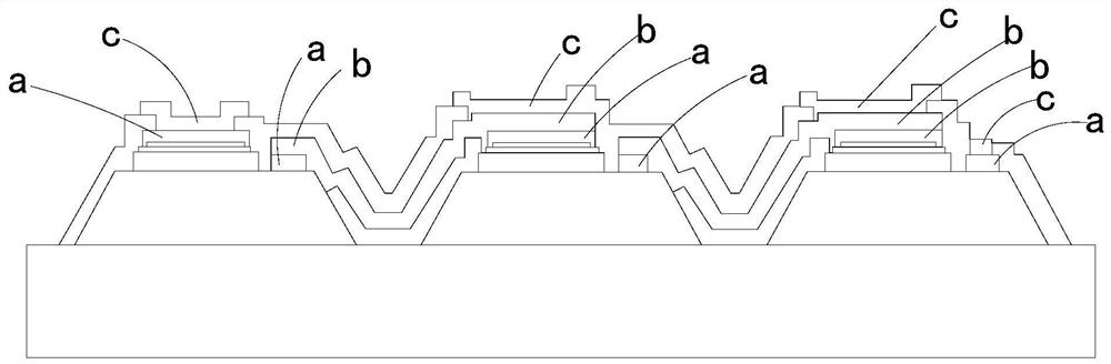
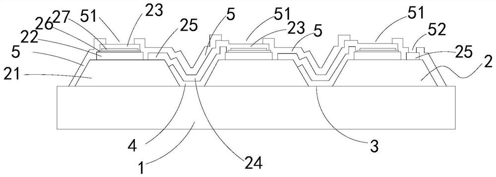
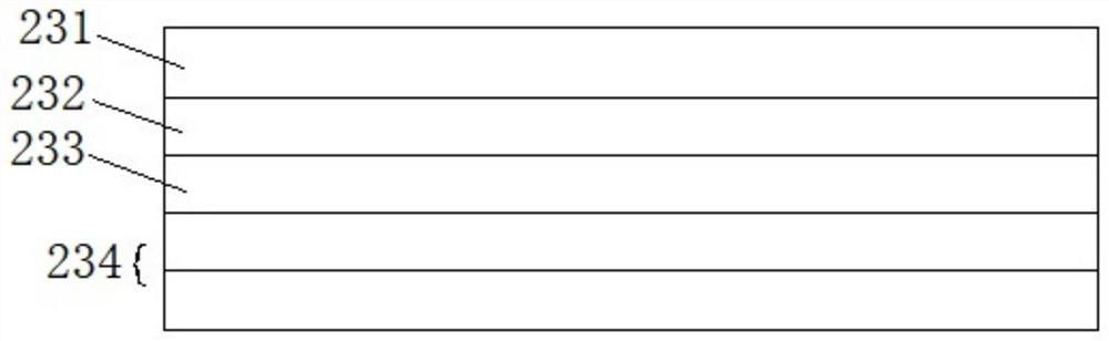
[0030] The specific implementation manners of the present invention will be further described in detail below in conjunction with the accompanying drawings and embodiments. The following examples are used to illustrate the present invention, but are not intended to limit the scope of the present invention.

[0031] In describing the present invention, it should be understood that the terms "center", "longitudinal", "transverse", "upper", "lower", "front", "rear", "left", " The orientation or positional relationship indicated by "right", "vertical", "horizontal", "top", "bottom", "inner", "outer", etc. is based on the orientation or positional relationship shown in the drawings, and is only for the convenience of description The present invention and simplified description do not indicate or imply that the device or element referred to must have a specific orientation, be constructed and operate in a specific orientation, and thus should not be construed as limiting the present...


PUM

PropertyMeasurementUnit
thicknessaaaaaaaaaa
thicknessaaaaaaaaaa
thicknessaaaaaaaaaa

Abstract

The invention relates to the technical field of LED chips, and discloses a flip LED chip, and the chip comprises a substrate and a plurality of GaN-based epitaxial layer units connected in series; each GaN-based epitaxial layer unit comprises an N-type GaN layer plated with an N-type electrode layer and a P-type GaN layer plated with a P-type electrode layer; the N-type electrode layer of the previous GaN-based epitaxial layer unit is connected with the P-type electrode layer of the next GaN-based epitaxial layer unit through a connecting electrode layer; each of the P-type electrode layer, the connection electrode layer and the N-type electrode layer comprises a Ti metal layer, a Ni metal layer or a Ni alloy layer, an Au metal layer and a SnAu-based alloy layer, wherein the Ti metal layer, the Ni metal layer or the Ni alloy layer and the Au metal layer are sequentially arranged from top to bottom, and the SnAu-based alloy layer is formed by arranging n Sn metal layers and n Au metal layers in a periodically staggered mode. According to the flip LED chip and the manufacturing method thereof, the number of electrode layers can be reduced, the production efficiency can be improved, meanwhile, the height difference between the positive electrode and the negative electrode is reduced, subsequent welding and heat dissipation of the chip are facilitated, the tin permeation resistance of the electrode layers is improved, and the internal structures of the electrode layers are firm.

Description

technical field [0001] The invention relates to the technical field of LED chips, in particular to a flip-chip LED chip and a manufacturing method thereof. Background technique [0002] The voltage of the blue LED is generally between 2.5V and 3.5V, while the mains voltage is 220V. Therefore, after the high-voltage chip connects the LED chips in series and parallel, the chip voltage increases to reduce the loss caused by voltage conversion. The integration of chips improves reliability, the arrangement of chips is denser, and the light intensity is more concentrated. [0003] Existing flip-chip high-voltage chips generally require a three-layer electrode structure, such as figure 1 As shown, one layer is the contact layer a, which is used to form a good ohmic contact with the epitaxial layer; one layer is the connection layer b, which is used to perform serial-parallel connections between chips; the last layer is a soldering layer used for welding and heat dissipation c. ...

Claims


Application Information

Patent Timeline
Patent Type & Authority Applications(China)
IPC IPC(8): H01L33/32H01L33/14H01L33/40H01L33/64
CPCH01L33/14H01L33/32H01L33/40H01L33/647
Inventor 黄剑锋
Owner GUANGDONG DELI PHOTOELECTRIC
Why Eureka
Try Eureka