

Method of manufacturing nitride semiconductor device
A technology of nitride semiconductor and manufacturing method, applied in semiconductor/solid-state device manufacturing, semiconductor device, transistor and other directions, can solve problems such as unavoidable deterioration and insufficient reduction of leakage current, and achieve the effect of avoiding deterioration
- Summary
- Abstract
- Description
- Claims
- Application Information
AI Technical Summary
Problems solved by technology
Method used
Image

Examples
Embodiment approach 1
[0028] figure 1 It is a cross-sectional view showing the nitride semiconductor device according to Embodiment 1 of the present invention. An AlN high-resistance buffer layer 2 having a layer thickness of 300 nm is provided on a SiC substrate 1 . A GaN electron transit layer 3 with a layer thickness of 1 μm is provided on the AlN high-resistance buffer layer 2 . Al on GaN electron transit layer 3 with a layer thickness of 25nm 0.2 Ga 0.8 N donating electron layer 4. in Al 0.2 Ga 0.8 A gate electrode 5 , a source electrode 6 and a drain electrode 7 are arranged on the N electron-donating layer 4 . In the AlN high resistance buffer layer 2, the carbon concentration is controlled to be 10 18 cm -3 above, with a ratio of GaN electron transit layer 3 and Al 0.2 Ga 0.8 The resistance value of the N-donating sublayer 4 is high.
[0029] Next, a method of manufacturing the nitride semiconductor device according to Embodiment 1 of the present invention will be described. As ...
Embodiment approach 2
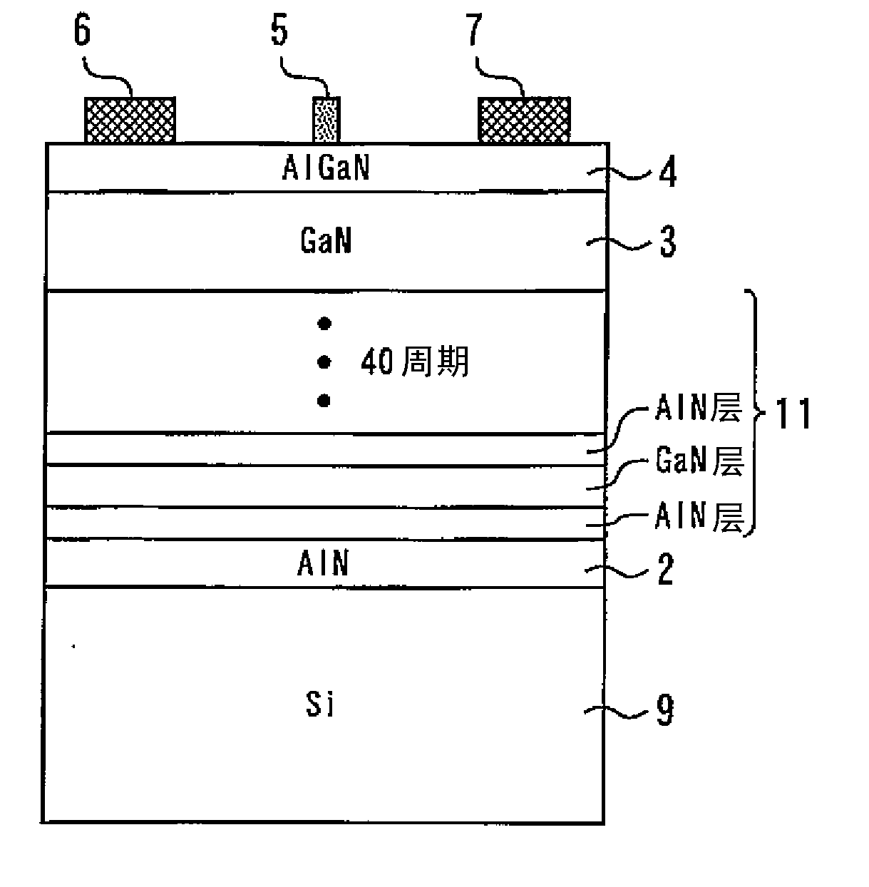
[0036] In Embodiment 2, when forming the AlN high-resistance buffer layer 2, UDMHy and NH 3 . The manufacturing method other than this is the same as that of Embodiment 1.
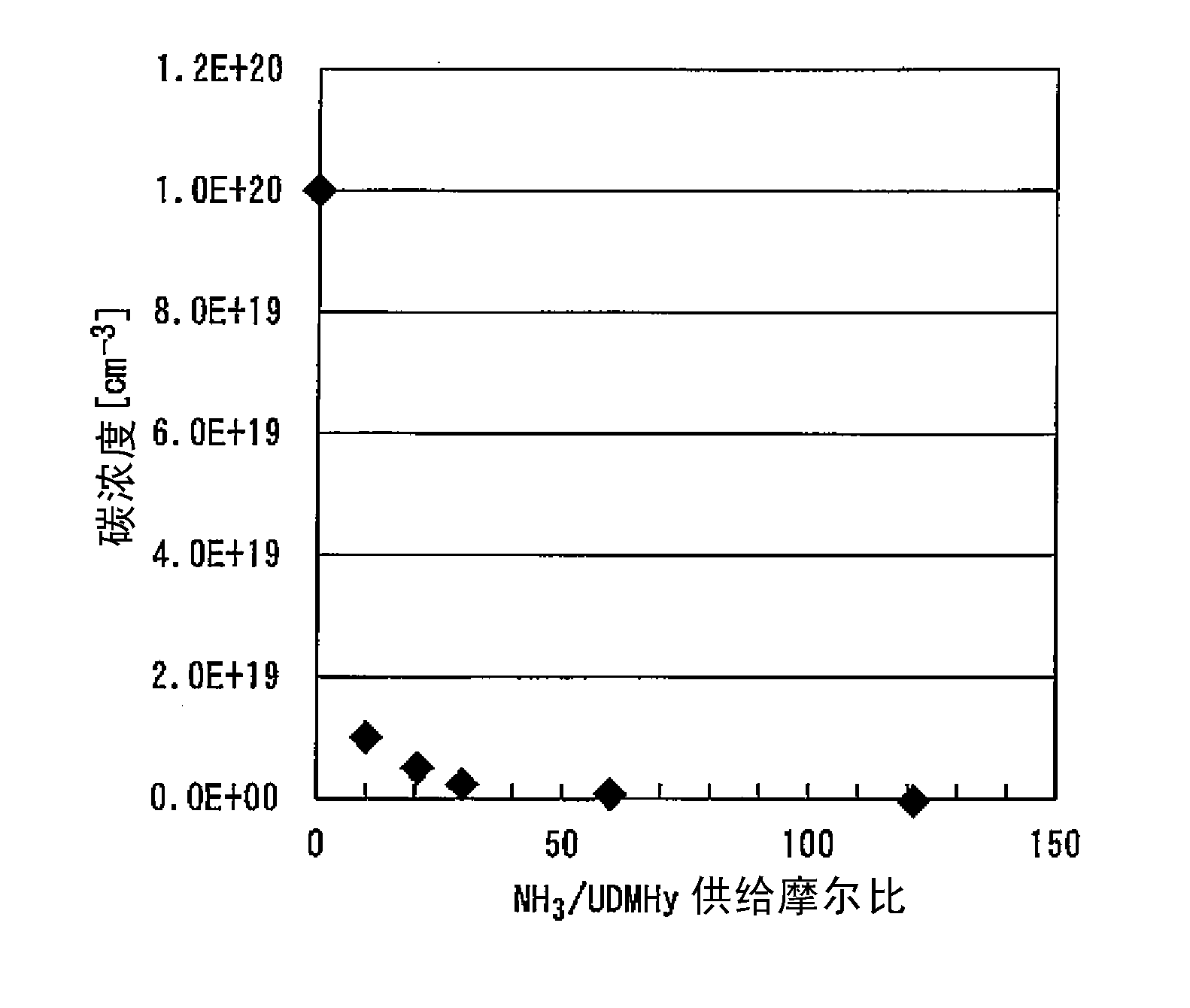
[0037] figure 2 is NH representing the carbon concentration 3 / UDMHy provides a plot of the molar ratio dependence. It can be seen from the figure that by making NH 3 The supply molar ratio to UDMHy is 30 or less, and the carbon concentration can be controlled to 10 18 cm -3 Above, without changing the growth temperature and growth pressure that affect the crystal quality. As a result, it can be obtained, for example, with 100Ωcm~1×10 7 The AlN high-resistance buffer layer 2 with the required resistivity of Ωcm, so the structure design becomes easy. Moreover, by changing the NH in the crystal growth 3 The / UDMHy supply molar ratio can also change the carbon concentration in the film thickness direction.
Embodiment approach 3
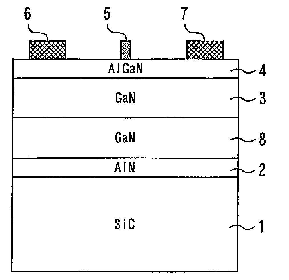
[0039] image 3 It is a cross-sectional view showing a nitride semiconductor device according to Embodiment 3 of the present invention. An AlN high-resistance buffer layer 2 having a layer thickness of 300 nm is provided on a SiC substrate 1 . A GaN high resistance buffer layer 8 with a layer thickness of 0.5 μm is provided on the AlN high resistance buffer layer 2 . GaN electron transit layer 3 having a layer thickness of 0.5 μm is provided on GaN high-resistance buffer layer 8 . Al on GaN electron transit layer 3 with a layer thickness of 25nm 0.2 Ga 0.8 N donating electron layer 4. in Al 0.2 Ga 0.8 A gate electrode 5 , a source electrode 6 and a drain electrode 7 are arranged on the N electron-donating layer 4 . In the AlN high-resistance buffer layer 2 and the GaN high-resistance buffer layer 8, the carbon concentration is controlled to be 10 18 cm -3 above, with a ratio of GaN electron transit layer 3 and Al 0.2 Ga 0.8 The resistance value of the N-donating sub...
PUM
| Property | Measurement | Unit |
|---|---|---|
| thickness | aaaaa | aaaaa |
| thickness | aaaaa | aaaaa |
| thickness | aaaaa | aaaaa |
Abstract
Description
Claims
Application Information