Method of manufacturing nitride semiconductor device

Inactive Publication Date: 2012-12-20
MITSUBISHI ELECTRIC CORP
View PDF3 Cites 7 Cited by
  • Summary
  • Abstract
  • Description
  • Claims
  • Application Information

AI Technical Summary

Benefits of technology

[0006]The present invention has been made to solve the above-described problems and it is an object of the present invention to provide a method of manufacturing a nitride semiconductor device capable of avoiding deterioration of crystal quality of a high-resistance buffer layer.
[0008]The present invention makes it possible to avoid deterioration of crystal quality of a high-resistance buffer layer.

Problems solved by technology

This necessarily leads to deterioration of crystal quality, such as resultant nitrogen holes, and leakage currents or the like cannot be sufficiently reduced.

Method used


Image

  • Method of manufacturing nitride semiconductor device
  • Method of manufacturing nitride semiconductor device
  • Method of manufacturing nitride semiconductor device

Examples


first embodiment

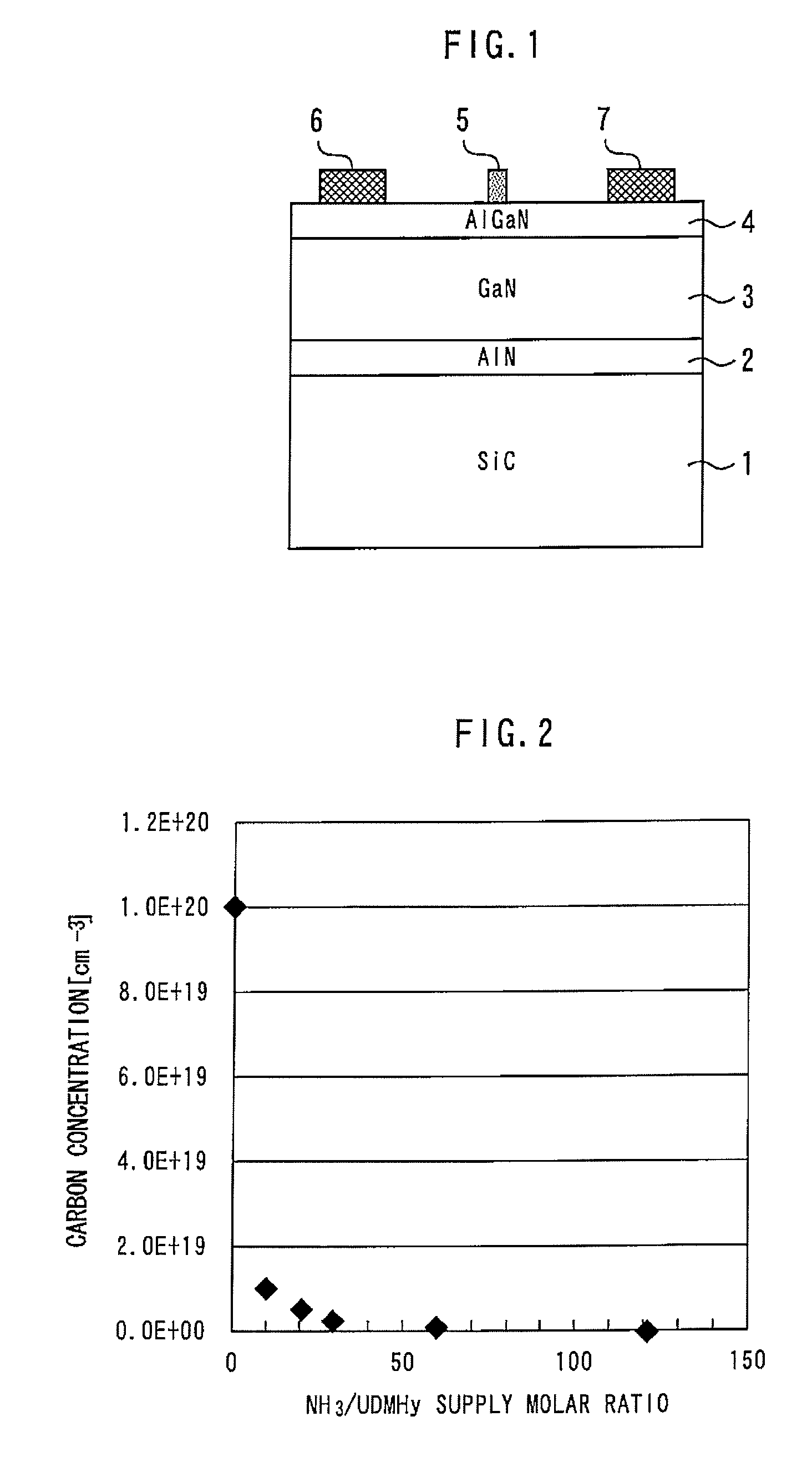
[0016]FIG. 1 is a cross-sectional view illustrating a nitride semiconductor device according to a first embodiment of the present invention. An AlN high-resistance buffer layer 2 having a layer thickness of 300 nm is provided on a SiC substrate 1. A GaN electron transit layer 3 having a layer thickness of 1 μm is provided on the AlN high-resistance buffer layer 2. An Al0.2Ga0.8N electron supply layer 4 having a layer thickness of 25 nm is provided on the GaN electron transit layer 3. A gate electrode 5, a source electrode 6 and a drain electrode 7 are provided on the Al0.2Ga0.8N electron supply layer 4. With carbon concentration controlled to 1018 cm−3 or above, the AlN high-resistance buffer layer 2 has a resistance value higher than the GaN electron transit layer 3 and the Al0.2Ga0.8N electron supply layer 4.

[0017]Next, a method of manufacturing a nitride semiconductor device according to the first embodiment of the present invention will be described. An MOCVD method is used as a...

second embodiment

[0021]A second embodiment uses UDMHy and NH3 as raw materials of group V when forming an AlN high-resistance buffer layer 2. The rest of the manufacturing method is the same as that of the first embodiment.

[0022]FIG. 2 is a diagram illustrating NH3 / UDMHy supply molar ratio dependency of carbon concentration. As is clear from this figure, by setting the supply molar ratio of NH3 with respect to UDMHy to 30 or less, it is possible to control the carbon concentration to 1018 cm−3 or above without changing the growth temperature or growth pressure which has influences on the crystal quality. As a result, the AlN high-resistance buffer layer 2 having desired resistivity within a range of, for example, 100 Ωcm to 1×10⁷ Ωcm can be obtained, and therefore the structure design can be made easier. By changing the NH3 / UDMHy supply molar ratio during crystal growth, it is also possible to change the carbon concentration in the film thickness direction.

third embodiment

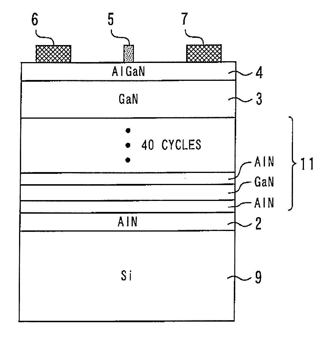
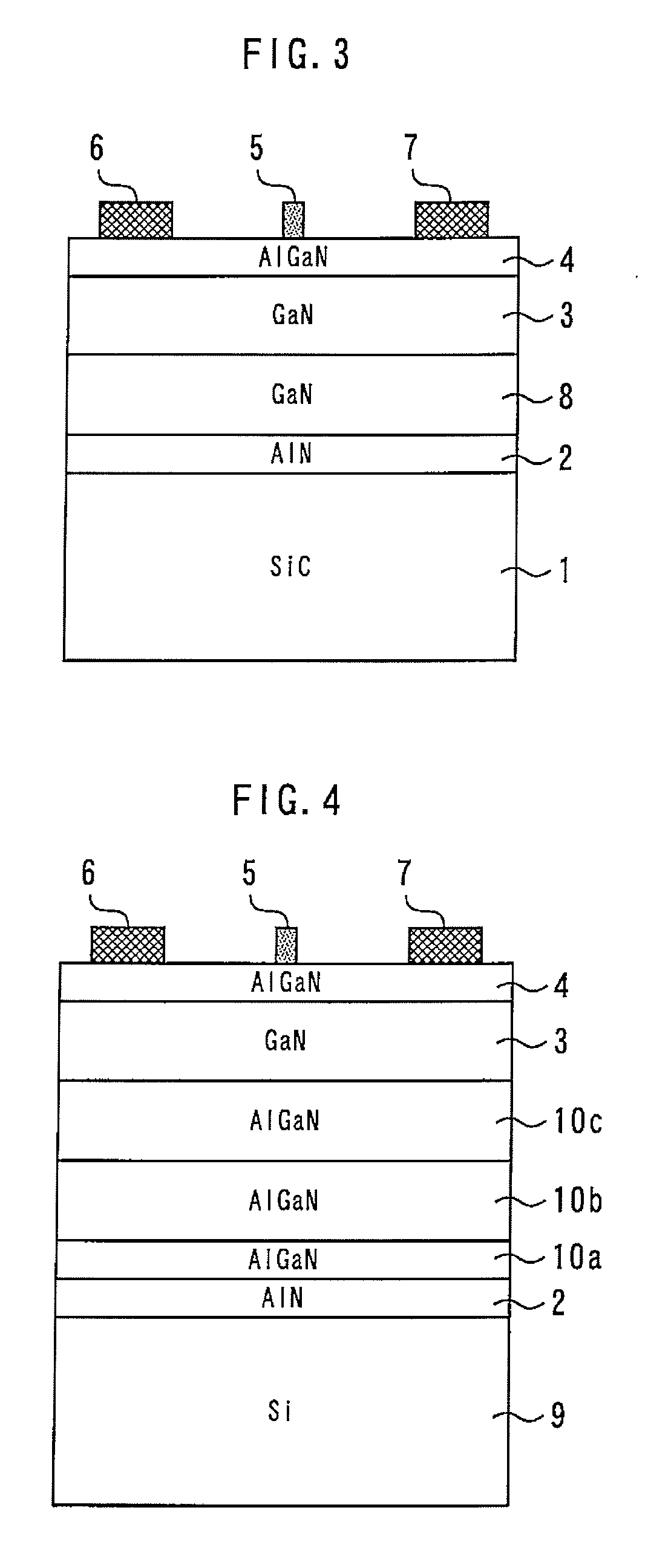
[0023]FIG. 3 is a cross-sectional view illustrating a nitride semiconductor device according to a third embodiment of the present invention. An AlN high-resistance buffer layer 2 having a layer thickness of 300 nm is provided on a SiC substrate 1. A GaN high-resistance buffer layer 8 having a layer thickness of 0.5 μm is provided on the AlN high-resistance buffer layer 2. A GaN electron transit layer 3 having a layer thickness of 0.5 μm is provided on the GaN high-resistance buffer layer 8. An Al0.2Ga0.8N electron supply layer 4 having a layer thickness of 25 nm is provided on the GaN electron transit layer 3. A gate electrode 5, a source electrode 6 and a drain electrode 7 are provided on the Al0.2Ga0.8N electron supply layer 4. Since the carbon concentration of the AlN high-resistance buffer layer 2 and the GaN high-resistance buffer layer 8 is controlled to 1018 cm−3 or above, these layers have higher resistance values than the GaN electron transit layer 3 and the Al0.2Ga0.8N ele...


PUM


Abstract

A method of manufacturing a nitride semiconductor device includes: forming a high-resistance buffer layer made of a nitride semiconductor having a carbon concentration of at least 1018 cm−3 on a semiconductor substrate by MOCVD, using an organic metal compound as a group III source material and using a hydrazine derivative as a group V source material; and forming a nitride semiconductor layer having a resistance lower than the high-resistance buffer layer on the high-resistance buffer layer.

Description

BACKGROUND OF THE INVENTION[0001]1. Field of the Invention[0002]The present invention relates to a method of manufacturing a nitride semiconductor device that forms a high-resistance buffer layer made of a nitride semiconductor on a substrate.[0003]2. Background Art[0004]Field effect transistors (FET) using a nitride semiconductor introduce a high-resistance buffer layer to reduce leakage currents in the buffer layer and improve a withstand voltage. A method of achieving high resistance by doping the nitride semiconductor with carbon as an impurity is proposed (e.g., see Japanese Patent Laid-Open No. 2000-68498, Japanese Patent No. 4429459 and Japanese Patent Laid-Open No. 2007-251144). A growth temperature, a growth pressure, a V / III ratio or the like is reduced in a MOCVD, thereby causing the doping of carbon from methyl radical, ethyl radical or the like of group III raw materials.SUMMARY OF THE INVENTION[0005]Conventional carbon doping methods reduce a growth temperature, a grow...

Claims


Application Information

Patent Timeline
IPC IPC(8): H01L21/20
CPCH01L21/02378H01L21/02458H01L21/02505H01L21/0254H01L21/0262H01L29/7787H01L29/1075H01L29/2003
Inventor OHNO, AKIHITO
Owner MITSUBISHI ELECTRIC CORP
Why Eureka
Try Eureka