AlGaN-based ultraviolet heterojunction phototransistor detector and preparation method thereof

A technology of phototransistor and detector, which is applied in the direction of semiconductor devices, circuits, electrical components, etc., can solve the problems that the structure of the device does not match the design requirements, the thickness of the main doping region is uncertain, etc., and achieve the elimination of adverse effects and reliable device operation Performance, Effect of High Epitaxial Crystalline Quality

Active Publication Date: 2019-01-29
SUN YAT SEN UNIV
View PDF4 Cites 9 Cited by
  • Summary
  • Abstract
  • Description
  • Claims
  • Application Information

AI Technical Summary

Problems solved by technology

[0006] However, even for an AlGaN-based HPT with a Collector-up structure, its collector p-n junction characteristics will still be affected by the Mg memory effect during epitaxial growth, that is, the memory effect makes the acceptor dopant Mg to the donor dopant. The impurity region (collector region) is diffused to compensate for impurities in the donor doped region (collector region), which leads to uncertainty in the actual thickness of the acceptor doped region (base region), and the problem that the device structure does not match the design requirements.

Method used


Image

  • AlGaN-based ultraviolet heterojunction phototransistor detector and preparation method thereof
  • AlGaN-based ultraviolet heterojunction phototransistor detector and preparation method thereof
  • AlGaN-based ultraviolet heterojunction phototransistor detector and preparation method thereof

Examples


Embodiment 1

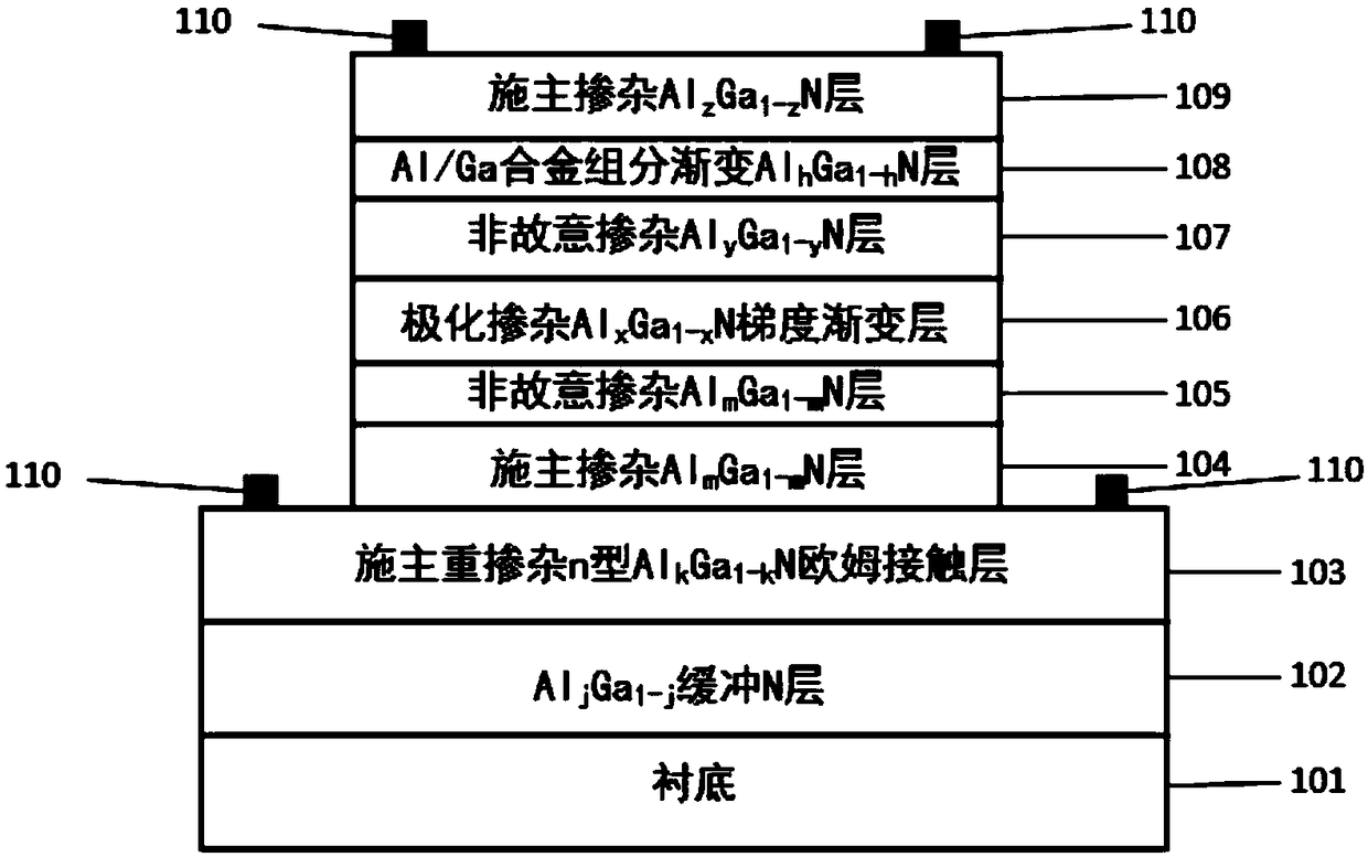
[0042] An AlGaN-based ultraviolet heterojunction phototransistor detector, such as figure 1 As shown, it is an npn-type structure, and the p-type base region is grown by polarized doping. The phototransistor detector includes a substrate 101 and an epitaxial layer grown on the substrate 101. The epitaxial layer includes sequentially from bottom to top Distributed buffer layer 102, n-type ohmic contact layer 103, donor-doped Al m Ga 1-m N layer 104, unintentionally doped with Al m Ga 1-m N layer 105, polarized doped p-type Al x Ga 1-x N gradient layer 106, Al y Ga 1-y N layer 107, Al with graded Al / Ga composition h Ga 1-h N layer 108, Al z Ga 1-z N layer 109 and distributed in ohmic contact layer 103 and Al z Ga 1-z The n-type ohmic contact electrode 110 on the N layer 109, wherein the starting value of the Al composition x≤m-0.1, and the ending value is y; m-0.4≤y≤m-0.2; the starting value of h is y, and the ending value is is z; y+0.1≤z≤y+0.2.

[0043] The prese...

Embodiment 2

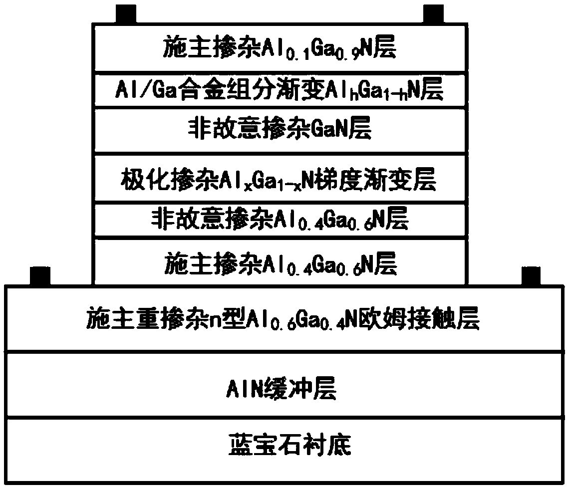
[0062] A kind of AlGaN-based ultraviolet heterojunction phototransistor detector described in this embodiment, such as figure 2 As shown, the npn structure is adopted, and the p-type base region is grown by polarized doping to provide the required carriers (holes). The phototransistor detector includes a c-plane sapphire substrate and an epitaxial layer, and the epitaxial The layer structure includes an AlN buffer layer with a thickness of 0.5 μm; a donor heavily doped n-type Al with a thickness of 1 μm 0.6 Ga 0.4N ohmic contact layer with an electron concentration of 3.5×10 18 cm -3 ; Donor-doped Al with a thickness of 100 nm 0.4 Ga 0.6 N layer with electron concentration of 1×10 18 cm -3 ; Thickness 10nm unintentionally doped Al 0.4 Ga 0.6 N layer; thickness 100nm polarized doped Al x Ga 1-x In the N gradient layer, the Al component is grown by a linear gradient, from a high Al component to a low Al component, and the Al component x=0.3~0, and the measured hole co...

Embodiment 3

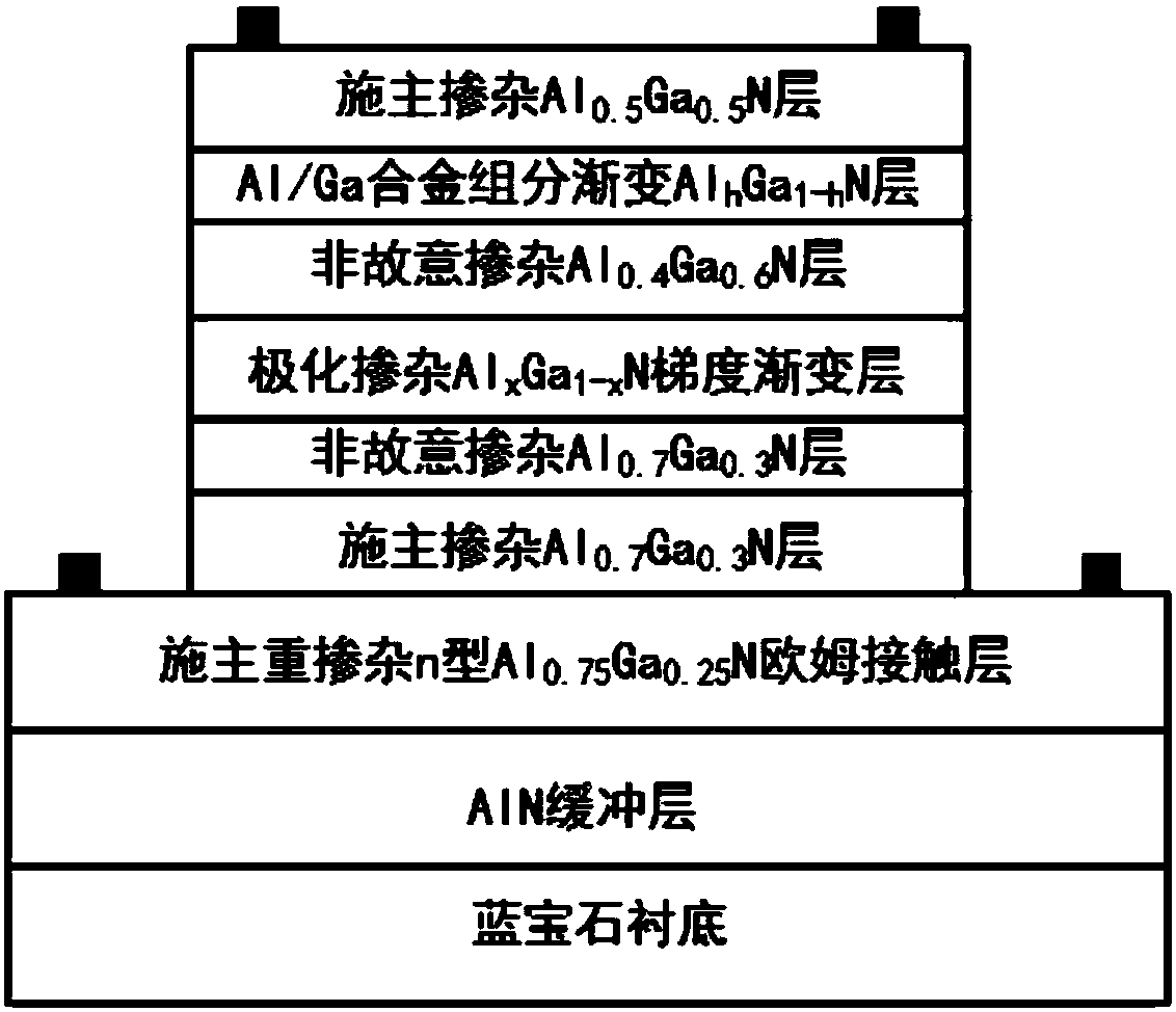
[0072] The phototransistor detector described in this embodiment is an AlGaN-based sun-blind ultraviolet heterojunction phototransistor, and its preparation method is basically the same as that of Example 1, the difference being that, as image 3 As shown, the structure of the epitaxial layer includes an AlN buffer layer with a thickness of 0.5 μm; a donor heavily doped n-type Al layer with a thickness of 1 μm 0.75 Ga 0.25 N ohmic contact layer with an electron concentration of 3.5×10 18 cm -3 ; Donor-doped Al with a thickness of 100 nm 0.7 Ga 0.3 N layer with electron concentration of 1×10 18 cm -3 ; Thickness 10nm unintentionally doped Al 0.7 Ga 0.3 N layer; thickness 100nm polarized doped Al x Ga 1-x In the N gradient layer, the Al component is grown by a linear gradient, from a high Al component to a low Al component, and the Al component x=0.7~0.4, and the measured hole concentration under the coherent growth condition is 3.6× 10 18 cm -3 ; Unintentionally dop...


PUM


Abstract

The invention relates to an AlGaN-based ultraviolet heterojunction phototransistor detector and a preparation method thereof. The AlGaN-based ultraviolet heterojunction phototransistor detector comprises a substrate and an epitaxial layer grown on the substrate, wherein the epitaxial layer comprises a buffer layer, an n-type ohmic layer, a donor doped AlmGa<1-m>N layer, an unintentionally doped AlmGa<1-m>N layer, a polarization doped p-type AlxGa<1-x>N gradient gradual change layer, an AlyGa<1-y>N layer, an AlhGa<1-h>N layer with the Al / Ga component gradually changing, an AlzGa<1-z>N layer andan n-type ohmic contact electrode distributed on the ohmic contact layer and the AlzGa<1-z>N layer, and the layers are sequentially distributed from bottom to top; the starting value of x of the Al component is less than or equal to (m-0.1), and the ending value is y, and y is greater than or equal to (m-0.4) and less than or equal to (m-0.2); and the starting value of h is y, the ending value isz, and z is greater than or equal to (y+0.1) and less than or equal to (y+0.2). The obtained transistor is good in design performance such as the crystal quality and high in reliability, and the obtained detector is excellent in photoelectric characteristic.

Description

technical field [0001] The invention relates to the technical field of group III nitride semiconductor ultraviolet photodetectors, in particular to an AlGaN-based ultraviolet heterojunction phototransistor detector and a preparation method thereof. Background technique [0002] With the continuous development of information technology, people's demand for detection and capture of external light information is increasing, and the requirements for light detection sensitivity are also increasing. Significant progress has been made in photoelectric detection from infrared, visible light to ultraviolet, and it is widely used in civil, industrial and military applications. Among them, ultraviolet detection is an important branch of light detection, covering UVC (100-280nm), UVB (280-320nm) and UVA (320-400nm) bands. It has important applications in fields such as halo discharge detection and missile tail flame detection. Traditional UV photodetection is mainly based on vacuum el...

Claims


Application Information

Patent Timeline
Patent Type & Authority Applications(China)
IPC IPC(8): H01L31/11H01L31/0304H01L31/18
CPCH01L31/03048H01L31/1105H01L31/1848Y02P70/50
Inventor 江灏孙李杰邱新嘉
Owner SUN YAT SEN UNIV
Why Eureka
Try Eureka