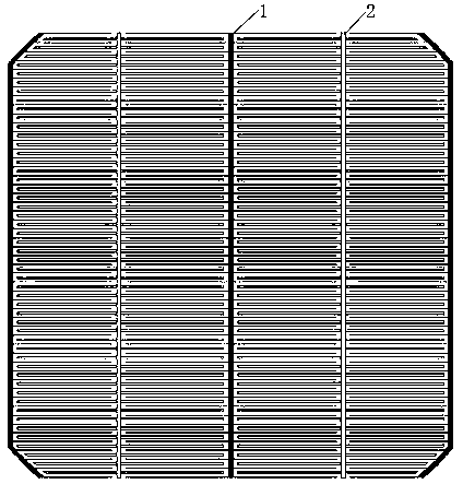
Preparation method of interdigitated back-contact battery based on N-type substrate
A substrate, N-type technology, applied in the field of solar cells, can solve the problems of difficult to control the uniformity of diffusion, decrease in the lifetime of the minority carrier of the silicon wafer, and great influence on the silicon wafer, and achieve the effects of good control, less pollution and uniform distribution.
- Summary
- Abstract
- Description
- Claims
- Application Information
AI Technical Summary
Problems solved by technology
Method used
Image

Examples
Embodiment 1
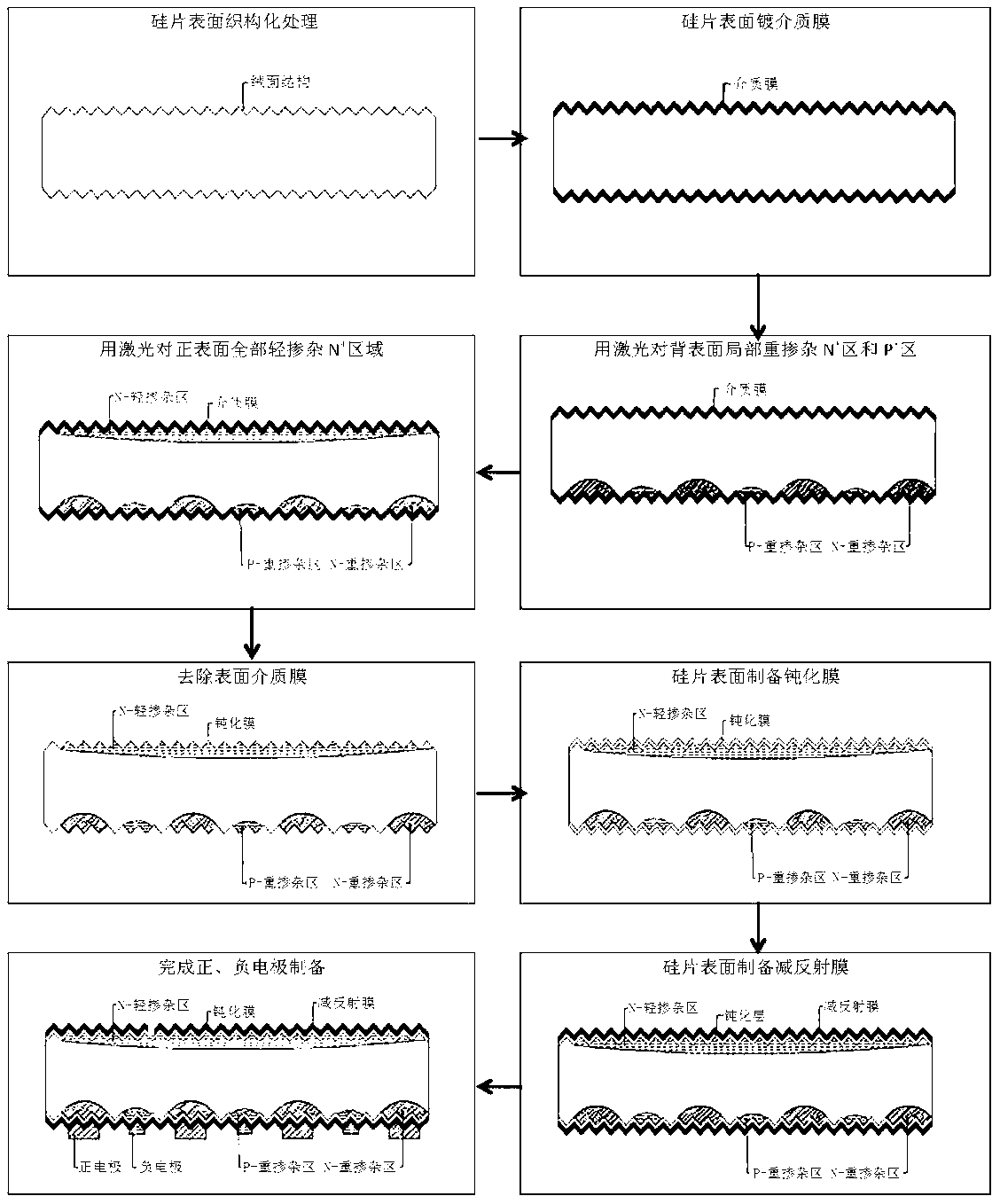
[0034] The present invention proposes a method for preparing an N-type IBC high-efficiency solar cell based on laser doping to prepare a back surface PN junction. The following takes an N-type monocrystalline silicon solar cell as an example, and the preparation steps are as follows:
[0035] ⑴Use a mixed aqueous solution of sodium hydroxide, IPA and texturing additives for N-type silicon wafers (wherein: sodium hydroxide mass fraction is 1.3%, IPA volume fraction is 0.3%, texturing additive volume fraction is 0.03%) for surface treatment , Make a uniform size pyramid-shaped suede structure; then use PECVD (plasma enhanced chemical vapor deposition) to prepare SiNx dielectric films on the front and back surfaces.
[0036] ⑵Spin-coating a phosphoric acid-ethanol mixed aqueous solution (phosphoric acid:ethanol:water=24:9:10) on the back surface of the silicon wafer; then use laser to perform partial N on the back surface of the silicon wafer + Heavy doping, using Paladin UV ultraviole...
Embodiment 2
[0043] (1) Carry out surface texture treatment on the crystalline silicon wafer, and prepare SiNx films on the front and back surfaces;
[0044] (2) On the back surface of the crystalline silicon coated with phosphoric acid, the partial N is prepared by scanning the AVIA green light with a wavelength of 532nm. + Heavy doped structure, clean and blow dry;
[0045] (3) Partial P is prepared on the back surface of crystalline silicon coated with boric acid by using AVIA green light scanning method with a wavelength of 532nm + Heavy doped structure, clean and blow dry;
[0046] ⑷Prepare N on the front surface of crystalline silicon coated with phosphoric acid by scanning AVIA with a wavelength of 532nm. + Lightly doped structure, and use 10% HF solution to clean the SiNx film on the front and back sides, and then clean and blow dry;
[0047] ⑸Using furnace tube dry oxidation method to deposit SiO on both sides of silicon wafer 2 membrane;
[0048] ⑹SiNx anti-reflection film is prepared on t...
Embodiment 3
[0052] (1) Carry out surface texture treatment on the crystalline silicon wafer, and prepare SiNx films on the front and back surfaces;
[0053] ⑵Prepare partial N on the back surface of crystalline silicon coated with phosphoric acid by using Paladin UV with a wavelength of 355nm. + Heavy doped structure, clean and blow dry;
[0054] (3) Partial P is prepared on the back surface of crystalline silicon coated with boric acid by using Paladin UV with a wavelength of 355nm. + Heavy doped structure, clean and blow dry;
[0055] ⑷Prepare N on the front surface of crystalline silicon coated with phosphoric acid by Paladin UV with a wavelength of 355nm. + Lightly doped structure, and clean the SiNx film on the front and back with a 10% HF aqueous solution, and then clean and blow dry;
[0056] ⑸Using furnace tube dry oxidation method to deposit SiO on both sides of silicon wafer 2 membrane;
[0057] ⑹SiNx anti-reflection film is prepared on the front and back sides of the silicon wafer;
[005...
PUM
| Property | Measurement | Unit |
|---|---|---|
| Resistance | aaaaa | aaaaa |
Abstract
Description
Claims
Application Information
 - R&D Engineer
- R&D Manager
- IP Professional
- Industry Leading Data Capabilities
- Powerful AI technology
- Patent DNA Extraction
Browse by: Latest US Patents, China's latest patents, Technical Efficacy Thesaurus, Application Domain, Technology Topic.
© 2024 PatSnap. All rights reserved.Legal|Privacy policy|Modern Slavery Act Transparency Statement|Sitemap