
Method for correcting offset of high-speed high-precision large-range low-power-consumption dynamic comparator
A technology of dynamic comparator and correction method, applied in the direction of analog/digital conversion calibration/test, etc., can solve the problems of limited accuracy, limited minimum capacitance value, nonlinearity, etc., and achieve the effect of low power consumption
- Summary
- Abstract
- Description
- Claims
- Application Information
AI Technical Summary
Problems solved by technology
Method used
Image

Examples
Embodiment Construction
[0030] The implementation method of the correction will be further described in detail in conjunction with the diagram below:
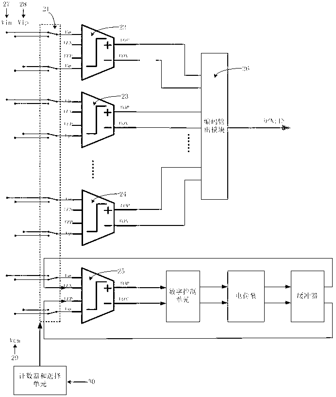
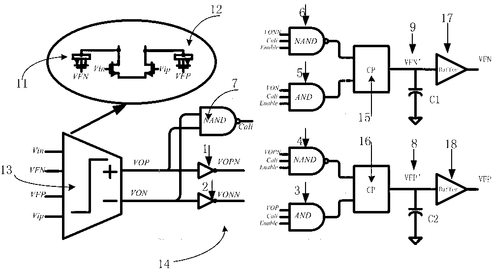
[0031] 1. The counter and switch selection array 30 sequentially selects a comparator (13) to be corrected from the comparator arrays 22, 23, 24, and 25, and connects the remaining comparators to the analog-to-digital converter according to the normal working mode among.
[0032] 2. The input terminal of the comparator to be corrected is connected to the common mode level VCM 29 and isolated from the input signal. Then the CKC high level comes, and the comparator is controlled for comparison. Although the input signal of the comparator is the same at this time, due to the existence of the offset voltage, the output terminal VOP or VON of the comparator will reach the logic low level (GND), and at the same time, because of the positive feedback of the latch structure, the other output terminal is forced to reach the logic level High level (VDD).
[...
PUM
 Abstract
Description
Claims
Application Information