A method of manufacturing a multilayer circuit board and the multilayer circuit board

A multi-layer circuit board, circuit board technology, applied in the direction of multi-layer circuit manufacturing, circuit, printed circuit, etc., can solve the problems of not completely avoiding pad connection failure, not fully compressing conductive paste, etc.

Inactive Publication Date: 2012-12-26
FUJITSU LTD
View PDF5 Cites 11 Cited by
  • Summary
  • Abstract
  • Description
  • Claims
  • Application Information

AI Technical Summary

Problems solved by technology

[0011] As mentioned above, since the conductive paste supplied to the via holes of the prepreg is not sufficiently compressed with the current method of manufacturing printed wiring boards, connection failures between pads are not completely avoided

Method used


Image

  • A method of manufacturing a multilayer circuit board and the multilayer circuit board
  • A method of manufacturing a multilayer circuit board and the multilayer circuit board
  • A method of manufacturing a multilayer circuit board and the multilayer circuit board

Examples


Embodiment Construction

[0025] [Multilayer PCB]

[0026] The following will refer to figure 1 , figure 2 , Figure 3A and Figure 3B Describe the construction of a multilayer circuit board.

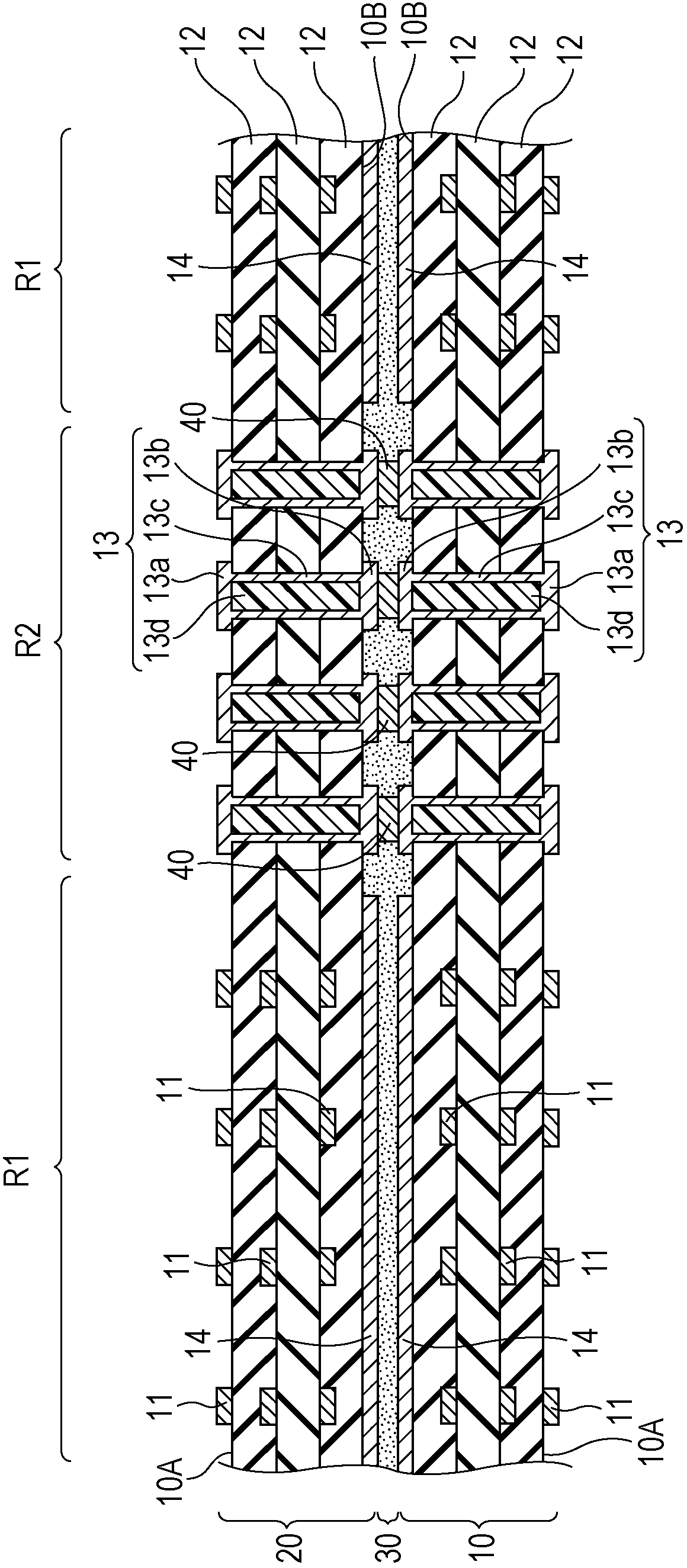
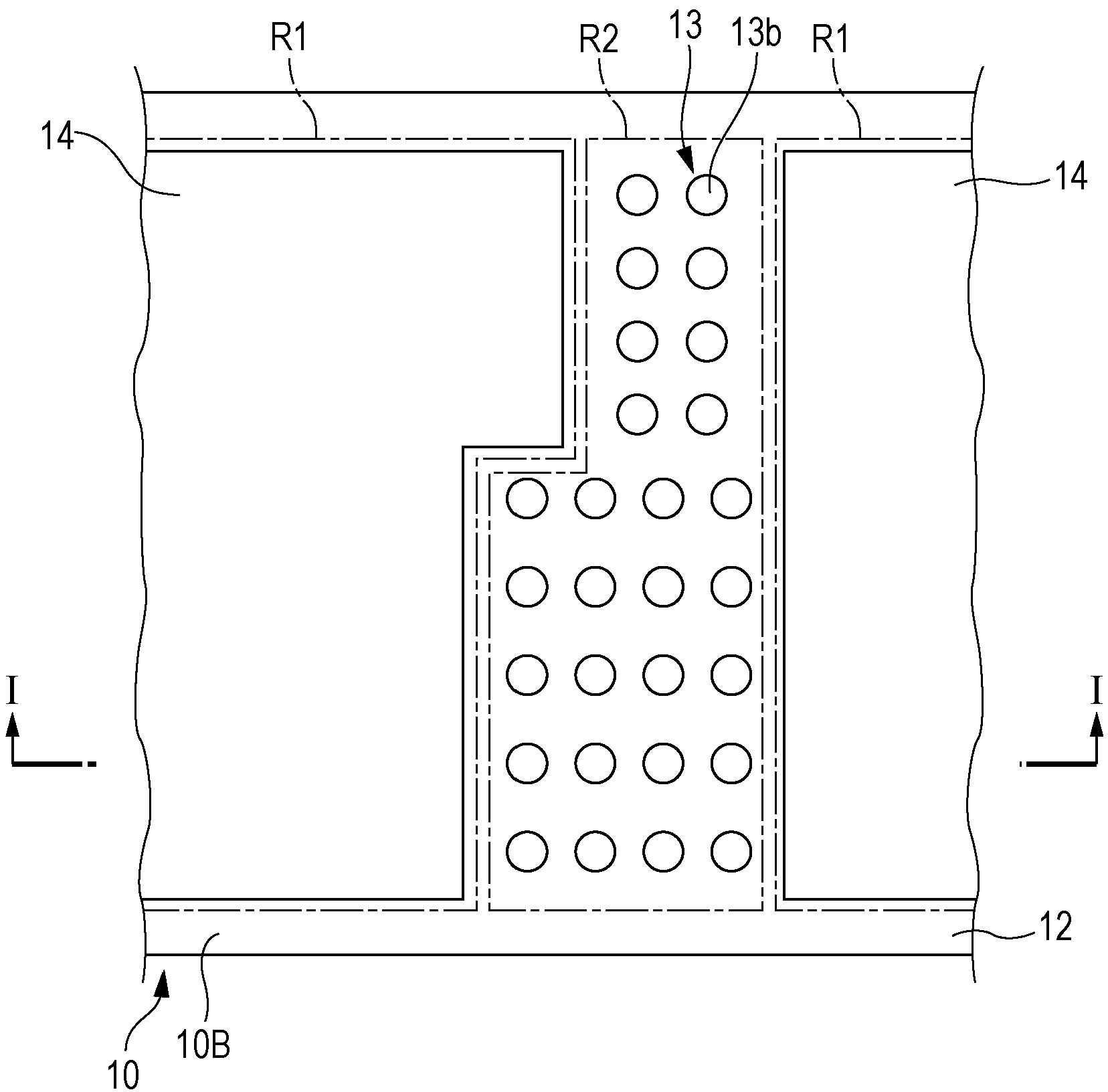
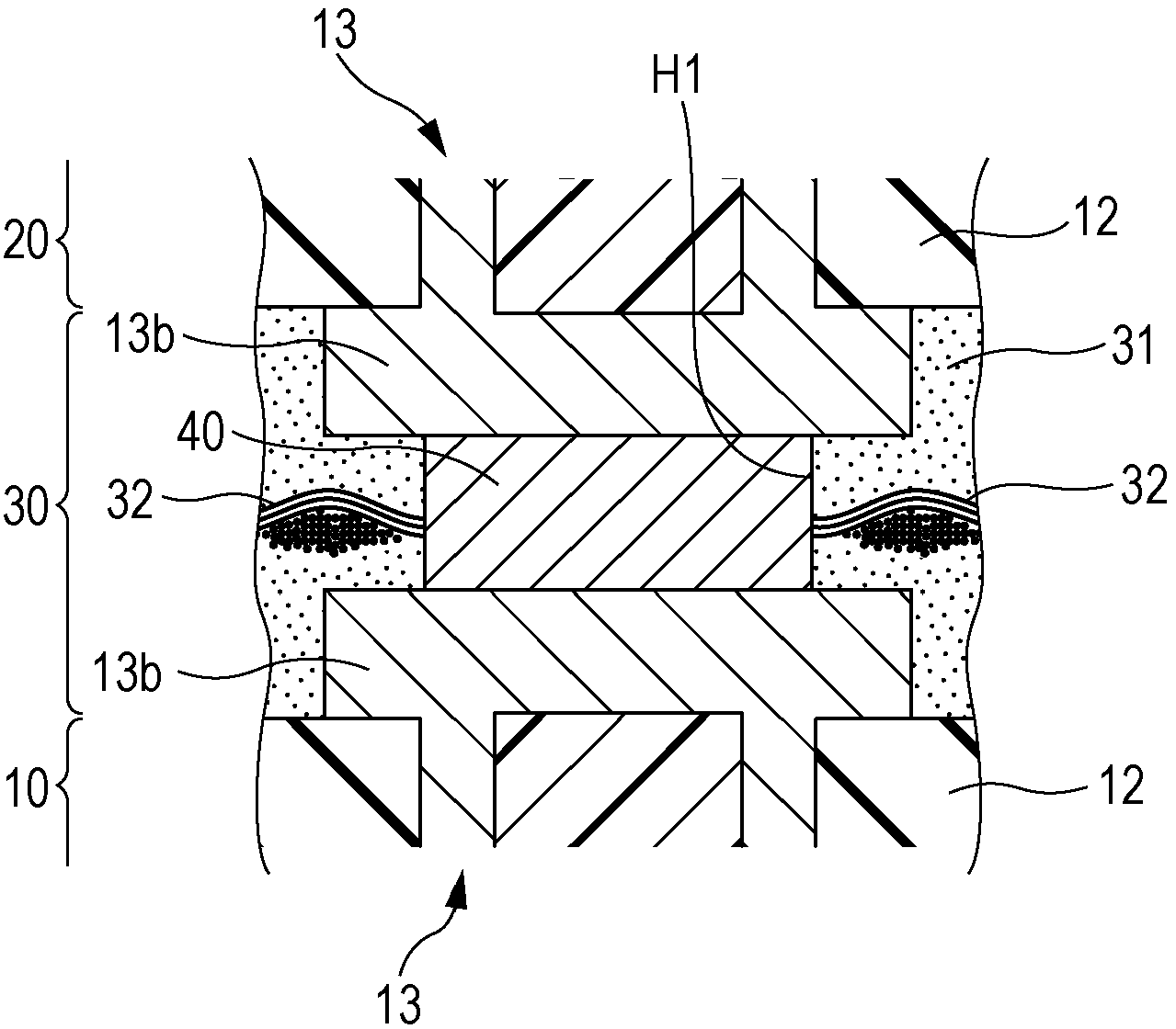
[0027] figure 1 is a cross-sectional view of a multilayer circuit board according to one embodiment. figure 2 is a plan view of the first circuit board 10 according to one embodiment, which depicts figure 1 In the second surface 10B of the first circuit board 10, the intermediate insulating layer 30 is bonded to the second surface 10B. To be careful of, figure 1 depicts along the figure 2 The cross section obtained in line I-I.

[0028] Such as figure 1 and figure 2 As shown, the multilayer circuit board includes a first circuit board 10, a second circuit board 20, an intermediate insulating layer 30 for bonding the first circuit board 10 and the second circuit board 20 to each other, and an intermediate insulating layer 30 for bonding the first circuit board 10 to each other. The pad connec...


PUM


Abstract

A method of manufacturing a multilayer circuit board includes forming a prepreg on a surface of a first circuit board including a first region in which a plated-through hole is formed and a second region in which a solid pattern is formed, the prepreg having a first hole reaching the plated-through hole and a second hole reaching the solid pattern, filling the first hole with a conductive paste, and pressing a second circuit board on the prepreg to laminate the first circuit board and the second circuit board to each other after filling the first hole with the conductive paste.

Description

technical field [0001] Embodiments discussed herein relate to a method of manufacturing a multilayer circuit board and the multilayer circuit board. Background technique [0002] In recent years, in printed circuit boards mounted in testing equipment such as semiconductor testers, increased wiring density is required as the number of terminals of semiconductor devices to be tested increases. In addition, in printed circuit boards used for communication equipment and servers, as the number of terminals of electronic parts to be mounted increases, an increase in wiring density is similarly required. [0003] As a technique for increasing the wiring density of a printed circuit board, a stacking technique of combining a plurality of wiring boards manufactured separately from each other into one printed circuit board has been proposed. [0004] In the method of manufacturing a printed wiring board by employing the above-described stacking technique, first, a prepreg serving as ...

Claims


Application Information

Patent Timeline
Patent Type & Authority Applications(China)
IPC IPC(8): H05K3/46H05K3/40H05K1/11
CPCH05K2201/0305H05K2203/061H05K3/46H05K3/40H05K3/4623H05K3/4614H05K3/4069H05K1/11H01L23/12H05K1/02
Inventor 吉村英明
Owner FUJITSU LTD
Why Eureka
Try Eureka