Method of producing circuit board

a technology of circuit board and production method, which is applied in the direction of resistive material coating, thermoplastic polymer dielectrics, printed circuit assembling, etc., can solve the problems of increasing the cost of producing circuit boards and increasing the cost of circuit boards, so as to reduce the cost of manufacturing processes

Inactive Publication Date: 2008-12-02
DENSO CORP
View PDF7 Cites 54 Cited by
  • Summary
  • Abstract
  • Description
  • Claims
  • Application Information

AI Technical Summary

Benefits of technology

[0017]In view of the foregoing and other problems, it is an object of the present invention to provide a method for producing a circuit board, in which a conductive paste in an insulating substrate is sintered to form a circuit conductor such that a resistance of a wiring pattern is low.
[0019]Accordingly, the conductive paste including the metal nano-particle can be sintered at the low temperature. Moreover, when the conductive paste is fired under the low-oxygen condition including the alcohol, the alcohol functions as a reducing agent. Thus, a surface oxide film of the metal nano-particle can be removed. That is, an increase in a resistance of the circuit conductor formed by sintering the conductive paste is prevented.
[0021]Accordingly, the forming of the multilayer wiring pattern and the sintering of the nano-particles can be performed at one time. Therefore, the manufacturing processes can be decreased extremely compared with conventional methods.

Problems solved by technology

The photolithography method has many processes and causes an increase in cost for producing the circuit board 90.
The multilayer by the build up method has many processes and causes an increase in cost for producing the circuit board.

Method used


Image

  • Method of producing circuit board
  • Method of producing circuit board
  • Method of producing circuit board

Examples


Embodiment Construction

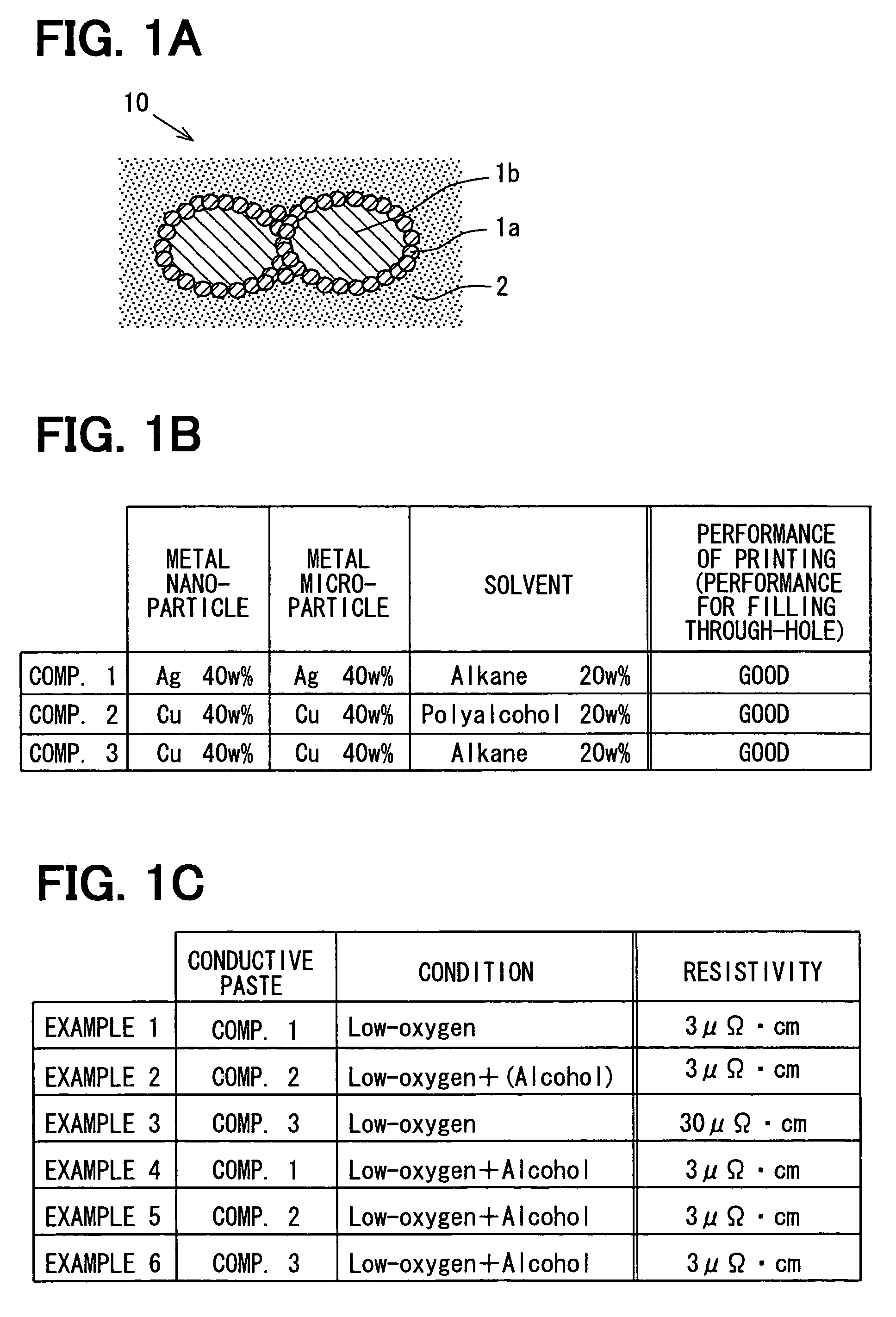
[0028]FIG. 1A is a pattern diagram showing component substances of a conductive paste 10 used in a method for producing a circuit board according to an embodiment of the present invention.

[0029]The conductive paste 10 shown in FIG. 1A includes metal nano-particles 1a whose diameters are nanometer orders. The diameter of the metal nano-particle 1a can be set equal to or less than 50 nm. In this case, the conductive paste 10 can be sintered at a low temperature equal to or less than 300° C., and elaborate wiring patterns and connecting conductors connecting the wiring patterns can be formed.

[0030]Further, metal micro-particles 1b are included in the conductive paste 10, as shown in FIG. 1A. The metal micro-particles 1b are made of the same metal as the metal nano-particles 1a, but the diameters of the metal micro-particles 16 are micrometer orders (e.g., several micrometers to tens of micrometers). A mixed material of the metal nano-particles 1a and the metal micro-particles 1b can re...


PUM

PropertyMeasurementUnit
diameteraaaaaaaaaa
diameteraaaaaaaaaa
temperatureaaaaaaaaaa

Abstract

A method of producing a circuit board includes a step of providing a conductive paste including metal nano-particles at an insulating substrate, and a step of sintering the conductive paste so as to form a circuit conductor. In the sintering step, the conductive paste is sintered in a low-oxygen condition including alcohol such that the metal nano-particles are sintered.

Description

CROSS REFERENCE TO RELATED APPLICATION[0001]This application is based on Japanese Patent Application No. 2005-236864 filed on Aug. 17, 2005, the disclosure of which is incorporated herein by reference in its entirety.BACKGROUND OF THE INVENTION[0002]1. Field of the Invention[0003]The present invention relates to a method of producing a circuit board, in which a conductive paste in an insulating substrate is sintered to form a circuit conductor.[0004]2. Description of Related Arts U.S. Pat. No. 6,228,467 (corresponding to JP-A-2000-38464) and JP-A-2002-299833 disclose methods for producing a circuit board, especially a multilayer circuit board having a multilayer wiring pattern. In this method, a conductive paste in an insulating substrate is sintered to form a circuit conductor.[0005]FIGS. 4A-4I, 5A and 5B are cross-sectional views showing a method for producing a multilayer circuit board 90 similar to that in the U.S. Pat. No. 6,228,467.[0006]Firstly, as shown in FIG. 4A, a resin f...

Claims


Application Information

Patent Timeline
Patent Type & Authority Patents(United States)
IPC IPC(8): H01K3/10
CPCH05K1/097H05K3/4617H05K3/4632H05K3/4069H05K2201/0129Y10T29/49163H05K2203/1131Y10T29/49155Y10T29/49126Y10T29/49165Y10T29/49128H05K2201/0266
Inventor TOTOKAWA, MASASHININOMIYA, YASUNORI
Owner DENSO CORP
Why Eureka
Try Eureka